Keywords
Millimeter-wave, substrate integrated waveguide, Butler Matrix, Three-ports, 5G, antenna array, radiation pattern
This article is included in the Research Synergy Foundation gateway.
Millimeter-wave, substrate integrated waveguide, Butler Matrix, Three-ports, 5G, antenna array, radiation pattern
An antenna with tracking capability is required in various applications, including 5G wireless communication in millimeter wave. However, in millimeter wave, high path loss arises, which increases quadratically with the frequency, ∝ f2, as defined by Friis’ law.1 To overcome this issue, beamforming and multiple-input, multiple-output (MIMO) systems are reported to be the key components of 5G systems that are to be deployed in 2020 and years to come.2–4 Multibeam antenna arrays automatically identify the most effective data delivery, while reducing interference for nearby users. Multibeam antenna arrays with passive beamforming are practically chosen due to their small size, low cost, and high gain.5–7
Butler Matrix (BM) is a well-known and simple design used for forming multiple beams with a linear array, where it can form orthogonal beams, and has a high beam crossover level. In this regard, a BM circuit has been found to be effective in developing alternative beams in various beam antenna-array systems.8–11 Since BM allows beam tracking for the selected users while suppressing unwanted signal, it has been identified as a preferred solution for 5G communication networks.12–13
However, due to the four hybrids, four phase shifters and two crossovers in the conventional BM, the transmission line adds undesired effects, such as insertion loss.14 Substrate integrated waveguide (SIW) technology has been widely utilized due to its simple feeding network and low insertion loss.15–17 The SIW can control the aperture width to ensure that the system is tightly coupled. A new generation of high frequency integrated circuits, the SIW, as a type of rectangular dielectric-filled waveguide produced in a planar substrate with arrays of metallic vias or slots to produce bilateral edge walls, is a good candidate for generating low sidelobe antenna arrays.
In this work, a low loss SIW hybrid coupler is to be designed by realizing bilateral edge walls which control the current flow. The BM is to be designed by connecting the hybrid coupler with two -90° phase shifters and one phase shifter of -180°, with the respective reference to get the accurate output phase shift. This matrix is advantageous as it circumvents the crossover design, which is commonly used in the conventional design. The diameter and the pitch of the SIW via-hole is to be carefully designed to control the coupling throughout the BM path, to get a promising return loss and minimum transmission amplitude. The structure should be compact and low loss, which makes the BM suitable to be used in the beamforming application for the millimeter wave at 28 GHz.
In this design, the substrate of Rogers R04350B, with a thickness of 0.254 mm, dielectric constant of 3.66 and loss tangent, (tan δ) of 0.0037, is chosen due to their excellent performance at higher frequencies. See underlying data18 for this section.
According to Mohd Shukor et al.,19 a lower loss tangent is required in the substrate to ensure low dielectric loss and low dielectric absorption.
Q-factor due to the dielectric, QD, is expressed in H. B. Jeon et al. (1) with a value of 302.56, where εeff, λ0 and αd are the effective dielectric constant, the wavelength in the air and the dielectric loss, respectively.
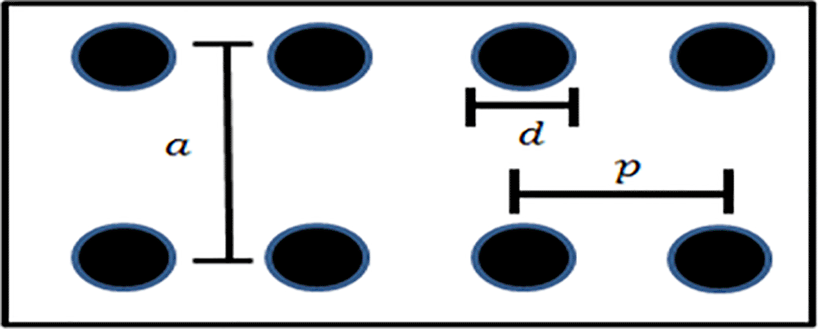
In the SIW configuration, an array of via holes is arranged in array configuration to create the mutual side walls and operate as a rectangular waveguide enabling the current to flow through it. Figure 1 shows the SIW structure, which has a via hole that is shorted in both planes to provide vertical current routes. Since these vertical metal fences are replaced by through via holes, the SIW propagation modes are comparable to those of rectangular waveguides.20–21 The SIW components in this segment have a via hole with a diameter of d and pitches of a and p, which represent the distance between the pairs of holes. With the optimized dimensions of the diameter and the pitches of the SIW into the coupler design, the proposed structure can fulfil the operational bandwidth at 28 GHz for millimetre wave.
As explained by Balanis,22 the resonance frequency was determined as shown in previous studies (2-4), where the width and length of the SIW cavity are appropriately optimized to accommodate the TE10 mode propagation. The SIW cavity's width and length are represented by weff and leff in the analysis:
Based on (5-6), pitch should be kept short to reduce the leakage loss between nearby holes, where d is denoted as the diameter and p as the pitch (the distance between centre to centre of adjacent via holes).
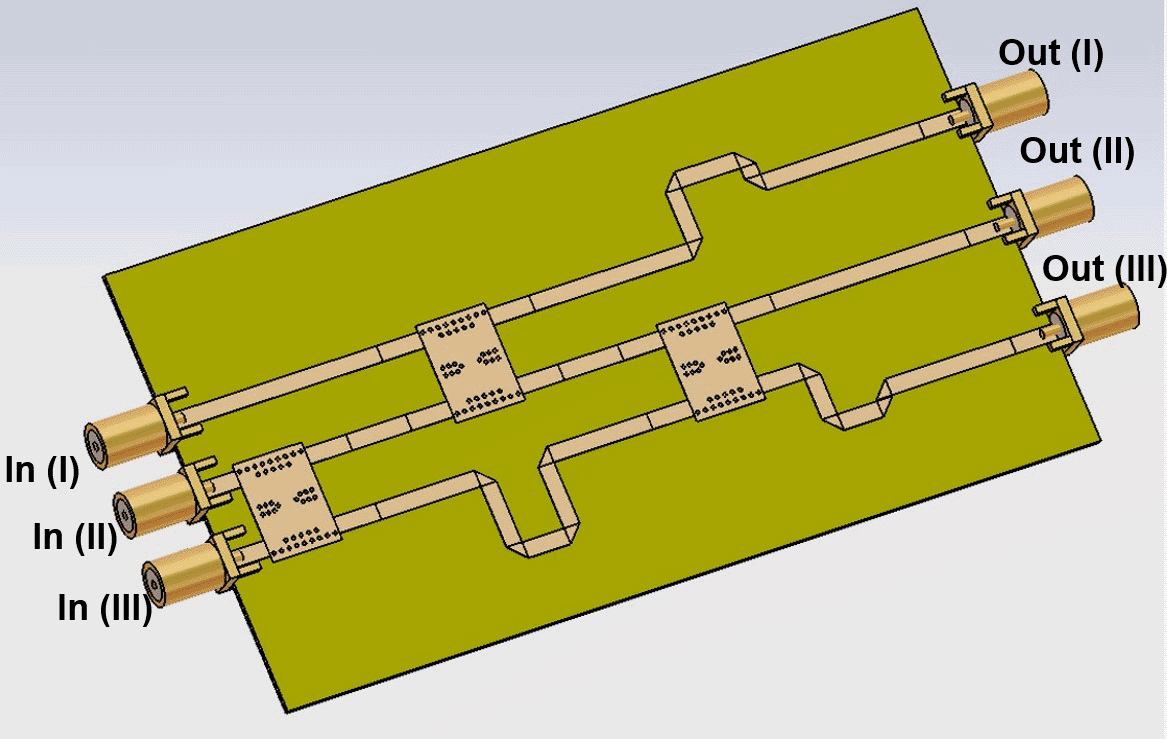
Figure 2 shows the signal path through three input and three output ports of the BM and Figure 3 (a), (b), and (c) illustrate the signal flow when the input is fed into In (I), In (II) and In (III), respectively. When the signal is fed into In (I), it passes through Coupler (II) and is divided into two outputs, where the first signal passes through Phase Shifter (I) producing an output signal of -180° at Out (I). The other signal passes Coupler (III) and Phase Shifter (III) producing an output signal of -180° at Out (II). The signal from Coupler (II) is coupled in Coupler (III) and produces an output of -180° at Out (III). The result obtained show the phase difference between these three output ports is 0°.
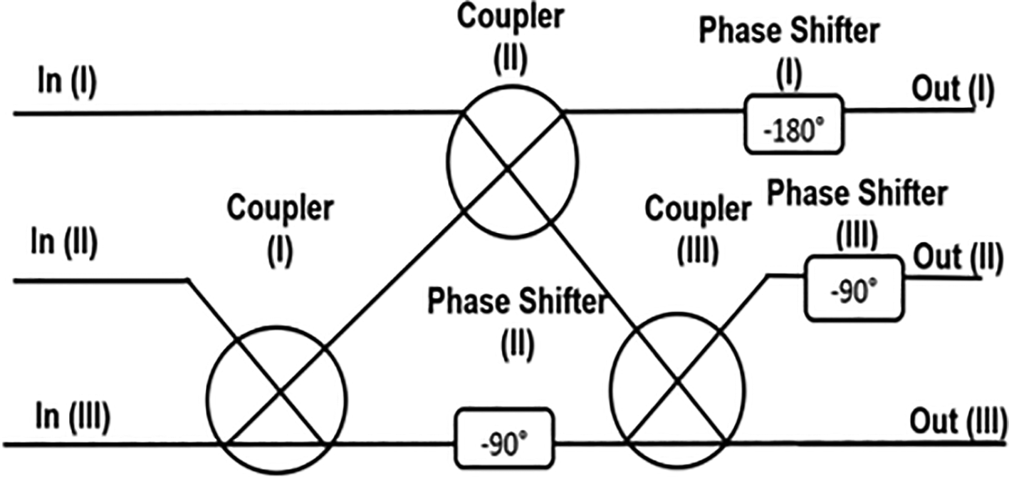

When the signal is fed into In (II), the signal passes to each of the couplers and passes through the phase shifter according to the signal path. The first signal produces an output signal of -270° at Out (I). The signals to Out (II) produces an output signal of -90° and -360°. The superposition of the two signal vectors (-90°, -360°) formed at output port Out (II), results in an output signal value of -30°. Similarly, the signal from In (II) to the Out (III) passes through two different paths, where the first signal produces an output signal of -90° while the other signal, results in an output signal of -180° at Out (III). The superposition of the signal vectors (-90°, -180°), results in an output signal value of -150°. Thus, the phase magnitude of the signals obtained at each output port when Port 2 is fed are -270°, -30° and -150°. The equal phase difference results obtained when In (II) fed is +120°.
The input signal fed to In (III), produces an output signal of -360° at Out (I) when it passes through Coupler (I), Coupler (II) and Phase Shifter (I). The superposition of the signal vector of - 180°, -270 results in an output signal value of -240° at Out (II). At Out (III), output signal of -120° is produced from the superposition of the signals (-180°, -90°). The phase magnitude of the signal obtained at each output port when In (III) is fed are -360°, -240° and -120°. The output phase difference obtained when Port 3 is fed is -120°.23
The design of the SIW hybrid couplers shown in Figure 4 (a) is conducted using electromagnetic software, Computer Simulation Technology (CST) (The open-source version of this software is available at CST STUDIO SUITE Student Edition | 3DEXPERIENCE Edu (3ds.com). The phase delay of the coupler signal is 90°, and this is due to the quarter wavelength line at the coupler branch with 50-ohm impedance. The signal flow is depicted in Figure 4 (b), where the input signal is equally split to each respective output ports. In this design, the W aperture dimension controls the value of the coupling to be 3 dB. When a signal is fed into Port 1, it is distributed uniformly to Ports 2 and 3, while Port 4 is isolated because it does not receive power. When all ports are matched, power entering Port 1 is evenly distributed across Ports 2 and 3, with a 90° phase shift between these outputs. No power is connected to Port 4, because the signal is out of phase.
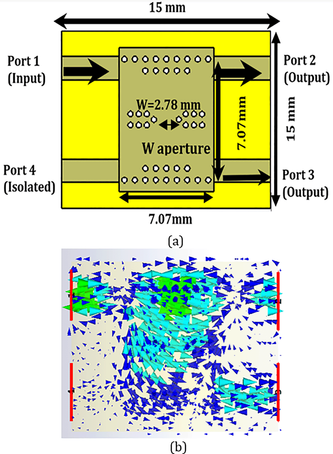
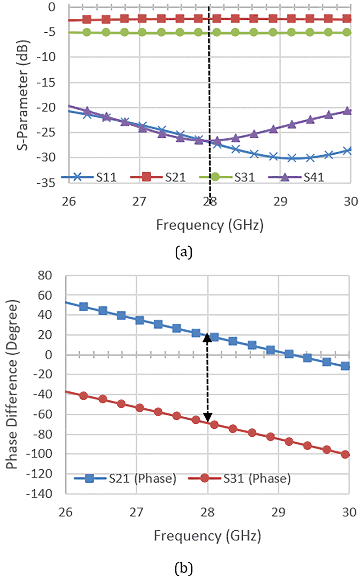
Equation (7) can be used to determine the coupling factor, where the W aperture dimension is 2.78 mm, the pitch is 1mm, and the diameter of the air hole is 0.3 mm. The results of the hybrid are shown in Figure 5 in terms of return loss, S11, insertion loss, S21, coupling, S31, isolation, S41, and output phase difference. The simulation shows that the values of -27.35 dB for return loss (S11), -3.9 dB for insertion loss (S21), -3.2 dB for coupling (S31) and -26.54 dB for isolation (S41) indicate a high transmission efficiency. The coupling factor implies that the output signal is distributed evenly between the output ports, and that the phase difference between the two output ports is 93 degrees. The coupling equation (7) is shown below:
The phase shifter is designed in the BM to control the output beams radiated by the patch antennas. Three phase shifters are designed with phase differences of -90° and -180°, as shown in Table 1. In reference to the structure, phase shifter I and phase shifter II are designed with the hybrid coupler as the reference, while phase shifter III is designed with the respective transmission line as the reference. Each length dimensions of the phase shifter is controlled to produce accurate phase difference between the output ports, ∡ (P (4,3)) and the input ports, ∡ ((P (2,1)) which are -180° and -90°, respectively. The width of the microstrip transmission line used in the phase shifter has width dimension of 0.7826 mm, indicates 50 ohms impedance. The matched impedance of the transmission line is used to prevent losses occurring when integrated with the antenna array feed.
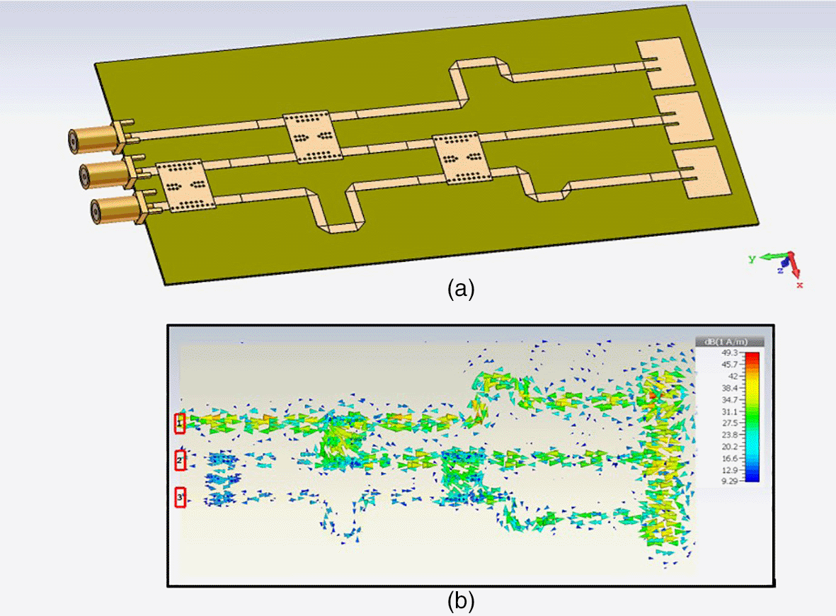
The proposed BM has a three input and three output matrices, where this system is designed to produce equal amplitude and phase at the output ports. Figure 6 illustrates the perspective view of the BM configuration, which has three elements for both the input ports and output ports. If the input ports are supplied with the signal, evenly distributed output signals are fed to each of the hybrid coupler and the phase shifter elements accordingly.
The phase shift between adjacent output ports, once the input port is fed with signal, δi in (8), is generated by:
For i = ± (1/2), ± (3/2), ± (5/2), ± (N-1)/2.
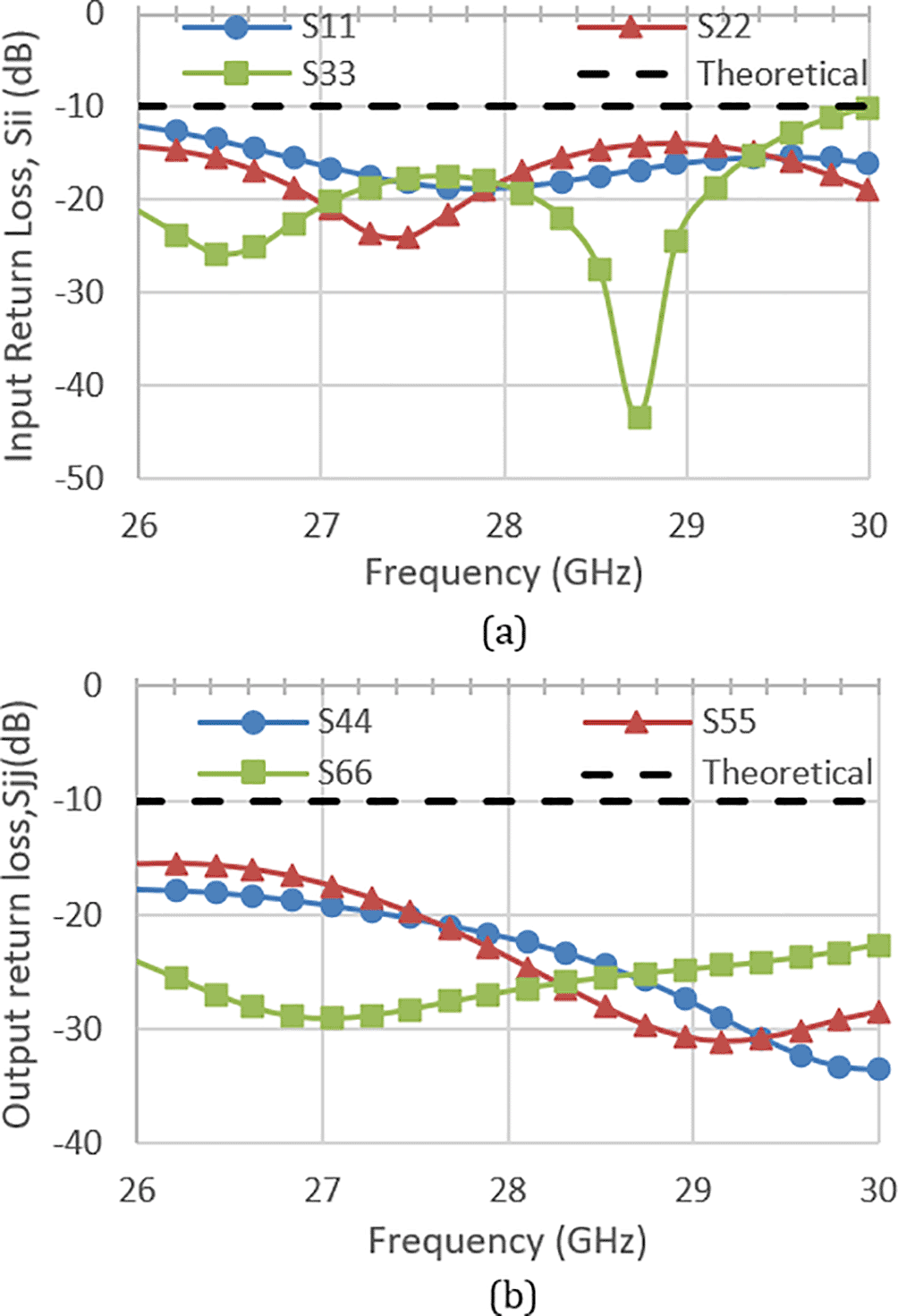
The performance of the 3 × 3 BM is studied using S-parameter simulation. The input and output return losses, Sii and Sii, are shown in Figure 7, where i represents the input ports and j represents the output ports. The results show that the return loss values are below -10 dB (theoretical) indicating a high transmission efficiency and the bandwidth fulfilling the requirement of the millimetre wave at 28 GHz (from f1 = 27.5 GHz, to f2 = 29.5GHz). The transmission amplitudes show values of –6 ± 3 dB for each Sij respective input-output port in Figure 8.

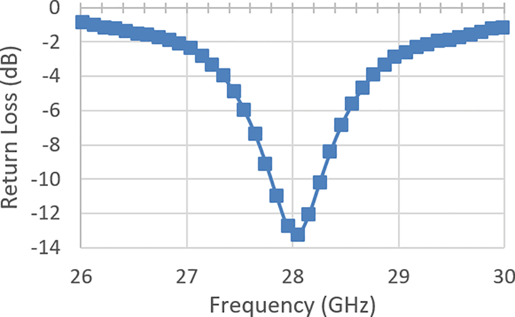
The SIW BM is connected to the planar antenna array to observe the radiation pattern. The element of the patch antenna is shown in Figure 9, where the dimensions are tabulated in Table 2. Figure 10 illustrates the return loss of the patch antenna at the interested bandwidth achieved below -10 dB. Three patch antennas are connected to the output of the BM, with λ0 /2 spacing between each other at 28 GHz, as illustrated in Figure 11 (a). When a signal is fed into the input ports, it is distributed with equal amplitude and progressive output phase shift to these three patch antennas. The antenna array spacing is set at λ0/2, which is equivalent to 5.357 mm at 28 GHz spacing, to provide a narrow beamwidth with reduced sidelobe.
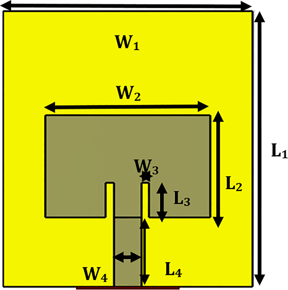
| Parameter | Dimension (mm) | Parameter | Dimension (mm) |
|---|---|---|---|
| W1 | 7.15 | L1 | 9.13 |
| W2 | 4.70 | L2 | 3.40 |
| W3 | 0.23 | L3 | 1.14 |
| W4 | 0.78 | L4 | 2.29 |
The amplitude and phase excitation of each phase array antenna element are separately controlled to produce a radiated beam to the specific angle. The proposed structure, as seen at the center frequency, provides an equal power split from each input port, i (#1, #2, #3), to all output ports, j (#4, #5, #6). The current distribution is illustrated in Figure 11 (b,) when the input signal is fed into Port 1 (#1). The array factor can be influenced by the number of antenna elements, layout configuration, magnitude, minimum spacing, and relative phase. Equation 9 provides the equivalent phase shift across element, and 10 provides the BM beam direction, where d is the antenna distance and λ is the wavelength:
Three beams with 0°, 30° and -30° beam directions are achieved by R. J. Maiiloux.24 The multibeam array antenna BM generates three different beams angles in its x-y plane, due to the progressive output from the BM. Figure 12 depicts the H-plane radiation patterns; when each of the three ports is fed individually, three beam outputs with maximum gains of 11.1 dBi, 9.06 dBi, and 10.4 dBi and angle directions of 0°, +27°, and -27° are generated.
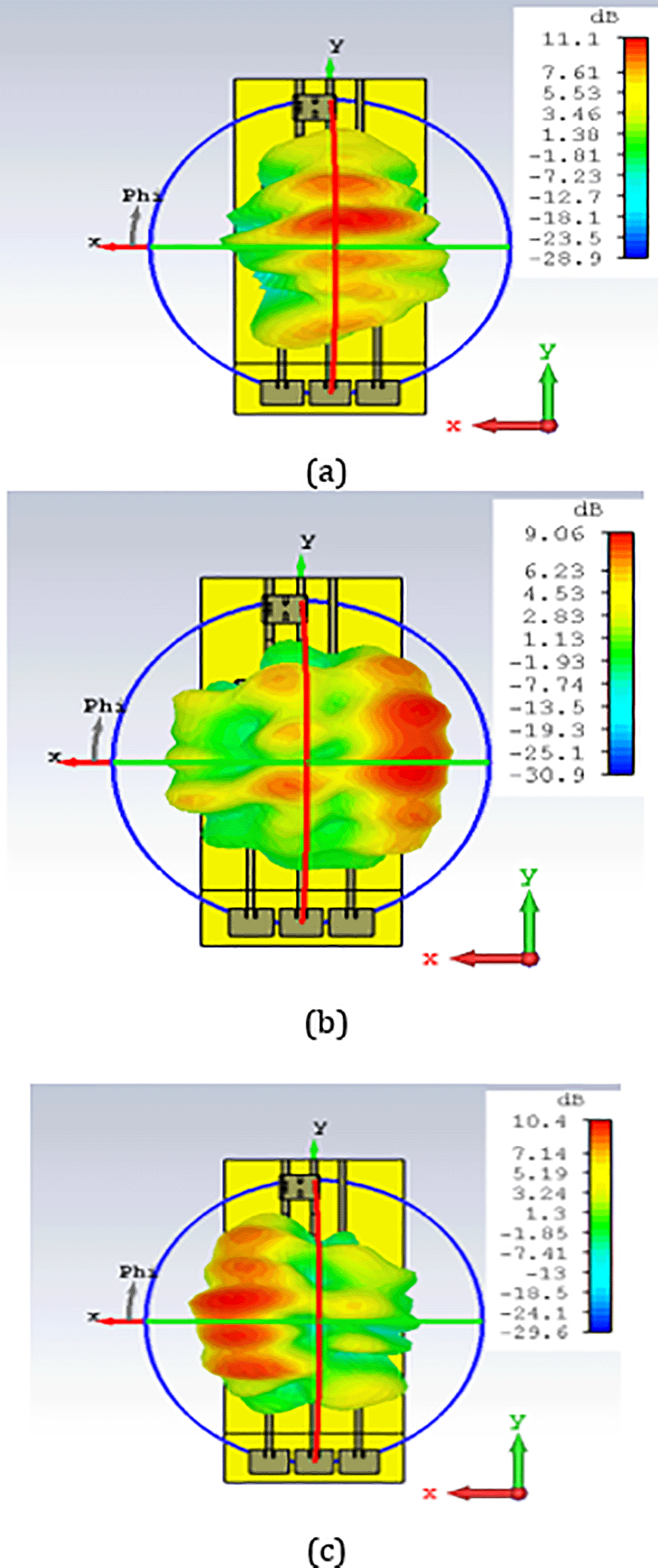
In this paper, the BM has been designed using the SIW technique, where the width aperture is used to control the coupling value. The 3 x 3 BM, which is small and compact, can be used to steer the beam to the selected users, when integrated with the antenna arrays. The simulation of the SIW BM with the patch antennas shows promising results in terms of the return loss, transmission amplitude, gain, and the radiation pattern, without any compromise on the size. The system develops three beams to the angles of 0°, + 27° and -27°, with respective gains of 11.1 dBi, 9.06 dBi, and 10.4 dBi. The beamforming network of the BM with antenna array has a compact size of (45.93×21.5) mm2. Because the system is small and low loss, it is suitable for placement in the base station of 5G communication networks.
Figshare: The data for the design of 5G Millimeter-Wave Beamforming System using Substrate Integrated Waveguide is listed.
DOI: https://doi.org/10.6084/m9.figshare.14883285.v218
This project contains the following underlying data:
• Data file 1. (Hybrid S-Parameter)
• Data file 2. (Hybrid S-Parameter (Phase))
• Data file 3. (BM Return Loss S-Parameter (a) input ports)
• Data file 4. (BM Return Loss S-Parameter (a) output ports)
• Data file 5. (BM Transmission Amplitude, Sij input port 1)
• Data file 6. (BM Transmission Amplitude, Sij input port 2)
• Data file 7. (BM Transmission Amplitude, Sij input port 3)
• Data file 8. (Patch Antenna S-Parameter)
Data are available under the terms of the Creative Commons Zero “No rights reserved” data waiver (CC0 1.0 Public domain dedication).
| Views | Downloads | |
|---|---|---|
| F1000Research | - | - |
|
PubMed Central
Data from PMC are received and updated monthly.
|
- | - |
Provide sufficient details of any financial or non-financial competing interests to enable users to assess whether your comments might lead a reasonable person to question your impartiality. Consider the following examples, but note that this is not an exhaustive list:
Sign up for content alerts and receive a weekly or monthly email with all newly published articles
Already registered? Sign in
The email address should be the one you originally registered with F1000.
You registered with F1000 via Google, so we cannot reset your password.
To sign in, please click here.
If you still need help with your Google account password, please click here.
You registered with F1000 via Facebook, so we cannot reset your password.
To sign in, please click here.
If you still need help with your Facebook account password, please click here.
If your email address is registered with us, we will email you instructions to reset your password.
If you think you should have received this email but it has not arrived, please check your spam filters and/or contact for further assistance.

 or whatever.
Comments on this article Comments (0)