Keywords
AIT, solar cells ternary (ABX₂), SCAPS.
This article is included in the Fallujah Multidisciplinary Science and Innovation gateway.
This article is included in the Solar Fuels and Storage Technologies collection.
AIT, solar cells ternary (ABX₂), SCAPS.
Renewable energy technologies are essential for meeting the world’s demand for sustainable power. Among various options, solar photovoltaics remain one of the most promising, yet their cost and efficiency continue to pose challenges (V.V. Tyagi, et al., 2013). Moreover, optoelectronic applications encompass a range of technologies, including photovoltaic converters, nonlinear optoelectronic devices, light-emitting diodes, and sensors (Kazmerski et al., 1977; Wagner et al., 1974; Elliott, 1974).
Chalcopyrite semiconductors (I–III–VI) have attracted attention due to their high absorption coefficients, tunable band gaps, and environmental compatibility (Sh et al., 2019; Hadi et al., 2019). Within this group, Silver Indium Telluride AgInTe2 (AIT) stands out as a promising absorber material due to its direct band gap (~1.0 eV), good carrier mobility, and stable crystalline structure (Hadi et al., 2025). Several methods have been utilized to synthesize thin films of I-III-VI compounds, such as flashing evaporation (Mostaque et al., 2022), one-source evaporation (Zhuang-Hao Zheng et al., 2019), molecular beam epitaxy (Horikoshi, 2019), and sputtering (Behrisch and Eckstein, 2007). AgInTe2 is a relatively new photovoltaic material and is occasionally used as an absorber layer in research. Currently, AIT solar cells with the structure AgInTe2/In2S3/TiO2/FTO have been reported in only a few scientific publications (Chopra et al., 2004). The deposition process using gold electrodes has been described in relevant literature (Nguyen and Ito, 2012; Joy et al., 2023). The reported efficiencies range from 0.5% to 1.13%. The main reasons for the low efficiency are low volatile organic compound (VOC) emissions and a low fill factor (FF), both of which may result from inadequate selection of window layers.
In heterojunction thin-film solar cells, the window layer typically forms a pn junction with the absorber layer (Bin Rafiq et al., 2020). To achieve high luminous flux, the window layer should have a large band gap, be thin, and have low series resistance. Therefore, selecting the right window layer material is crucial for the effectiveness of a photovoltaic cell (Lilhare and Khare, 2020). Aluminum antimonide (AlSb), a group III-V compound, has a band gap of 1.6 eV at 300 K (He et al., 2011). It has the potential to replace the window layer in a thin-film photovoltaic cell that uses AIT technology. Furthermore, AlSb possesses two key properties: a dielectric constant of 10.9 at radio frequencies and an index of refraction of 3.3 at the wavelength of 200 nm (Seeger and Schonherr, 1991). Several methods, including co-evaporation, co-sputtering, and hot-wall epitaxy, can be used to deposit AlSb thin films (Feifei et al., 2006). However, AlSb has not yet been used with AgInTe2-based solar cells.
To achieve the pp+ structure, the back surface field (BSF) consists of a heavily doped layer with the same doping type as the absorber material. The presence of the BSF layer can improve spectral response, increase short-circuit current, and decrease contact resistance. An obstacle to minority-carrier mobility within the absorbing layer is the doping-level difference between the BSF and absorber layers (Hemmani et al., 2017). Barium silicate (BaSi2) has a bandgap ranging from 1.1 to 1.35 eV, making it highly suitable for solar applications (Morita et al., 2006). Additionally, because Barium (Ba) and Silicon (Si) are abundant in the earth, BaSi2 can be used to produce an affordable dual-heterojunction solar cell (Zhao et al., 2009). Therefore, BaSi2 shows excellent promise as a BSF layer material for advancing high-efficiency thin-film heterostructure photovoltaic cells, as Moon stated in 2020 (Moon et al., 2020). Several methods have been used to deposit BaSi2 thin films, including vapor-phase epitaxy, molecular beam epitaxy, and solid-phase epitaxy. Researchers like Hara (2016), Deng (2018), Du (2015), and Fomin (2017) have contributed to this field. Currently, there is no existing documentation on how BaSi2 can be employed as the BSF layer in conjunction with an AIT-based photovoltaic cell. This work demonstrates progress in developing an innovative thin-film photovoltaic cell with a double-heterojunction (DH) structure, using AIT as the material. The AlSb layer functions as the n-window, the AgInTe2 layer as the p-absorber, and the BaSi2 layer as the p+-BSF.
The output of dual-heterojunction (DH) solar cells has been proposed as a means to enhance solar cell efficiency (Almansouri et al., 2015). The Shockley-Queisser (SQ) efficiency limit for a dual-heterojunction solar cell ranges from 42% to 46%, according to De Vos (1980) and Brown and Green (2002). Hence, there is a possibility of enhancing efficiency by utilizing a DH framework. This study aims to improve the performance of an n-AlSb/p-AgInTe2/p+-BaSi2 thin films solar cell through numerical simulations using the Solar Cell Capacitance Program (SCAPS-1D). The effects of layer thickness and material parameters on photovoltaic efficiency were systematically analyzed, and an optimized configuration with improved conversion efficiency was proposed.
In this study, we used the powerful numerical simulation tool SCAPS-1D to simulate and evaluate AIT solar cells. SCAPS-1D can be used to detect and elucidate the physical phenomena in photovoltaic devices. All SCAPS-1D simulations used AM-1.5 spectral intensity (100 mW/cm2) as the standard test condition (STC). We analyzed in detail the effect of the thickness of the absorber window, and back surface field layers on the fundamental parameters of the solar cell. By adjusting the values of the input variables, we obtained optimal parameter values that improve the performance of the solar cell. The following Poisson and continuity equations for holes and electrons are used in SCAPS-1D numerical simulation calculations (Burgelman et al., 2000; Burgelman et al., 2004).
Simulation is a crucial method for comprehensively understanding the physical functions of solar cell systems, verifying the feasibility of proposed physical explanations, and assessing the impact of changes in physical structure on their efficiency. Several simulation models are currently available for simulating solar cells, such as SCAPS and AMPS. SCAPS (Solar Capacitor Simulator) is a simulation tool developed by solar cell researchers at the Institute of Electronics and Information Systems, Ghent University. It simulates a one-dimensional structure with seven semiconductor input layers.
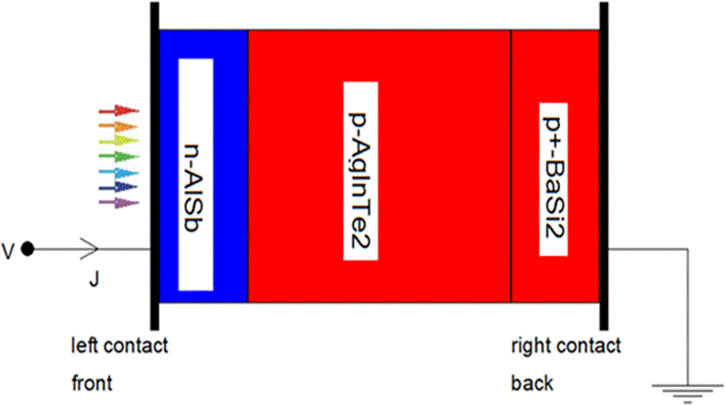
Unlike methods that analyze the properties and functions of each layer in detail to optimize solar cell performance, this method focuses on minimizing potential risks, time costs, and expenses (Pan and Zhu, 2016). Niemegeers (2014) provides a detailed description of the software and algorithms used. Figure 1(a) shows the solar cell design based on the AIT/CdTe structure in our case study. Figure 1(b) shows a schematic diagram and band structure of a double heterojunction solar cell based on AgInTe2 chalcopyrite. AgInTe2 is a p-type semiconductor with a specific optical band gap of 1.03 electron volts (eV). Its electron affinity is 3.6 eV, and its ionization energy is 4.63 eV. This material can be used as a thin film layer to absorb solar radiation. Figure 2 shows the structure of the thin film layer and the optical path into the simulated cell. To perform a simulation using SCAPS, we need to input specific physical parameters, including thickness, band gap (Eg), electron affinity (χ), relative permittivity (εr), density of states (NC, NV), and carrier mobility (μ). Table 1 lists these input parameters.
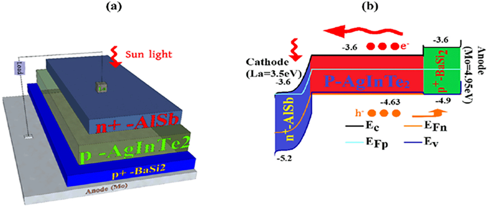
(a) Physical layer arrangement showing window, absorber, and BSF layers. (b) Corresponding band alignment illustrating charge transport pathways under illumination.
| Defects at various interfaces: | |
|---|---|
| Heterointerfaces | Defect density (cm−2) |
| AgInTe2/BaSi2 | 1.00 × 10¹⁰ |
| AlSb/AgInTe2 | 1.00 × 10¹⁰ |
The effective electron and hole masses, along with their mobilities, are obtained from the literature (Singh, 2001). The densities of states at the valence-band maximum (Nv) and the conduction-band minimum (Nc) can be calculated using Equation (3), as proposed by (Benseddik et al., 2022).
The symbol for m*e/p denotes the effective band masses of electrons and holes, where h represents Planck’s constant and k represents the Boltzmann constant. The velocity at which electrons move due to thermal energy:
The contact barrier for a p-type semiconductor is represented as FBp, whereas the affinity for electrons χ sc is calculated using Formula (3) as described by Benamara (2022).
Where Wm is the metal’s work function, and the FBp value is obtained from the literature (Patel, 1995).
In the SCAPS-1D simulation, all calculations were performed under AM1.5G illumination (100 mW/cm2, 300 K). The simulation considered recombination at interfaces and within bulk layers, using defect densities listed in Table 1. The optimization was conducted by systematically varying the layer thicknesses of AlSb (0.1–0.5 μm), AgInTe2 (0.2–1 μm), and BaSi2 (0.1–1 μm). Each parameter set was iteratively solved until convergence (Δη < 10−4). The metal contact work functions were 5.0 eV (front) and 4.6 eV (back), ensuring ohmic behavior. All material parameters were verified using previous studies (Benseddik et al., 2022; Chen et al., 2018; El-Korashy et al., 1999).
The output characteristics of a photovoltaic (PV) cell consist of the current in the short circuit density (JSC), the voltage of the open circuit (VOC), the fill factor (FF), as well as efficiency (η). rely on the carrier concentration and defect density of different layers, such as the window, absorber, and back surface field (BSF) layers, as well as the thickness of these layers. The maximum output of the AIT solar cell has been determined by improving its device construction.
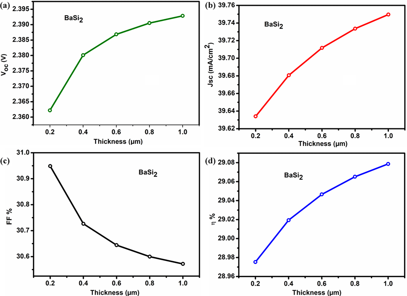
This section investigates the impact of the AIT semiconductor layer on the photovoltaic performance of AlSb/AIT/BaSi2 solar cells. The absorber layer thickness ranged from 0.2 to 1 μm. Table 1 shows the uniformity of width, doping concentration, and bulk defects in the window layer and back field layer. Figure 3 illustrates the photovoltaic (PV) performance as a function of absorber layer thickness. This figure shows the relationship between absorber layer thickness and efficiency: as the thickness increases, exciton generation increases, thereby improving efficiency. Increasing the absorber layer thickness increases the absorption of longer wavelengths of light, resulting in a larger number of electron-hole pairs. Decreasing the absorber layer thickness brings the depletion region closer to the back field contact, allowing it to receive more electrons for recombination. Reduced electron participation in the generation process leads to lower fill factor and efficiency. The electric field significantly affects the fill factor; as the reverse bias voltage increases, the fill factor in the absorber layer decreases.
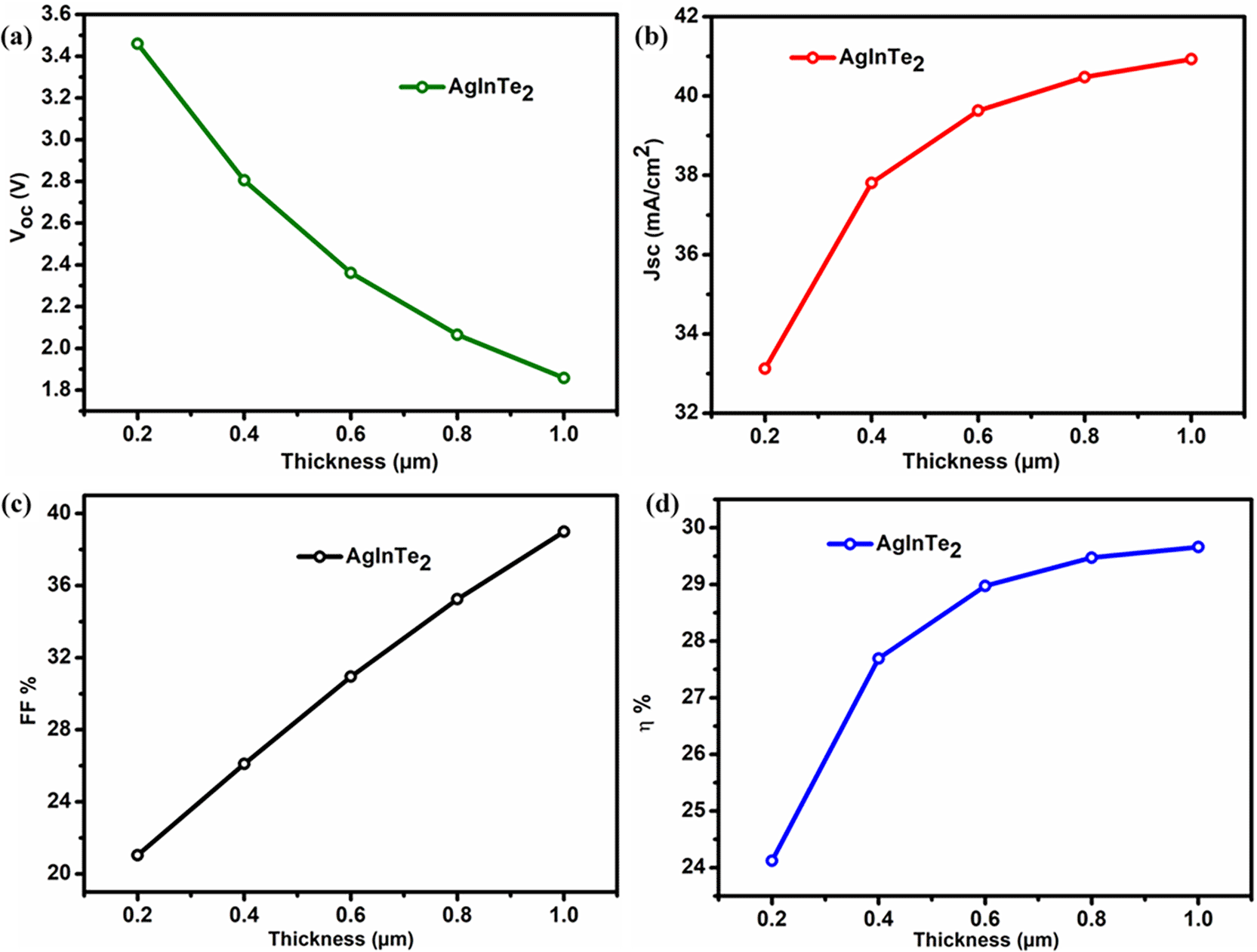
The optimal efficiency occurs near 1 μm.
This leads to a decrease in carrier yield, which is further exacerbated by the electric field. The Voc/thickness plot shows that increasing thickness increases the open-circuit voltage, but the numerical effect is small. According to the Jsc/thickness plot, increasing the thickness increases the short-circuit current. This is because greater thickness increases spectral sensitivity at longer wavelengths; the optimal absorber layer thickness is 1 μm. The highest power conversion efficiency at this thickness is 29.66%, with Jsc = 40.93 mA/cm2, Voc = 1.85 V, and FF = 38.99%.
The thickness of the AlSb layers was systematically varied from 0.1 to 0.5 μm to examine the correlation between the AlSb window layer and its width. Figure 4 demonstrates the influence of modifying the thickness of the window’s layer on the photovoltaic characteristics of the AlSb/AIT/BaSi2 photovoltaic cell. Increasing the AlSb layer width reduces both JSC and PCE. This effect arises from increased parasitic absorption, which impedes the penetration of shorter-wavelength photons into the absorbing layer. The upper and lower limits of the current density for JSC range from 43 to 30 mA/cm2. The highest attainable efficiency of 32% is achieved with an initial thickness of 0.1 μm, and it decreases to 23% with a thickness of 0.5 μm.
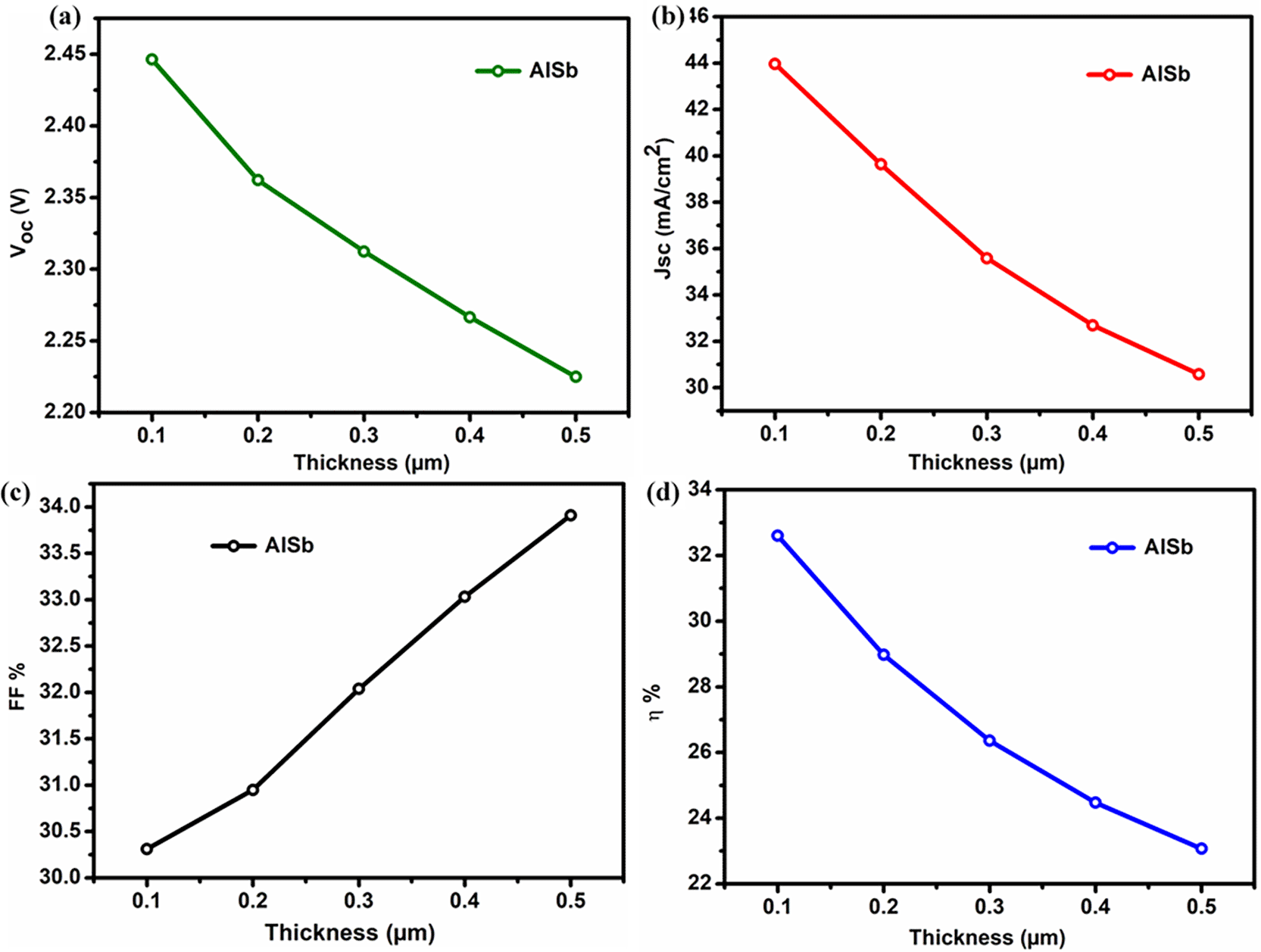
Thinner AlSb layers enhance photon transmission and current density.
In contrast, the variation in the length of the window’s layer has little influence on the values of VOC (voltage at open circuit) and FF (fill factor).
The photovoltaic capabilities are minimally affected by the depth of the window layer due to the robust carrier mobility and wide bandgap combination (Hossain, 2021).
This section presents a comprehensive investigation of the impact of the BaSi2 BSF layer on the performance of the AlSb/AIT/BaSi2 photovoltaic device. The width of the BaSi2 BSF layer has a slight impact on the solar photovoltaic performance of the AlSb/AIT/BaSi2 photovoltaic cell, as shown in Figure 5. Slight changes in the output parameters were seen when the thickness was modified. Nevertheless, increasing the thickness of BaSi2 could adversely affect photovoltaic (PV) performance. The increase in BSF thickness directly correlates with the rise in series resistance (Khattak et al., 2019).
Excessive BSF thickness increases series resistance, lowering overall efficiency.
To highlight the advancement achieved in this work, Table 2 compares the simulated results of the proposed device with earlier experimental and numerical studies on AgInTe2-based solar cells. The data clearly indicate a significant improvement in conversion efficiency and current density, mainly due to the optimized double-heterojunction structure and the use of AlSb and BaSi2 as window and BSF layers, respectively.
| Remarks | Structure | Jsc (mA cm−2) | Voc (V) | FF (%) | Efficiency (%) | Reference |
|---|---|---|---|---|---|---|
| Printed thin-film cell | AgInTe2/In2S3/TiO2/FTO | 20.3 | 0.45 | 50.1 | 0.50 | Nguyen & Ito (2012) |
| Numerical study | AgInTe2/ITO | 27.8 | 0.68 | 61.3 | 1.13 | Joy et al. (2023) |
| SCAPS simulation | AgInTe2/CdS | 32.0 | 0.72 | 62.0 | 2.30 | Benseddik et al. (2022) |
| Optimized DH Structure | AlSb/AgInTe2/BaSi2 | 43.9 | 2.40 | 30.3 | 32.6 | This Work |
This research examines the working mechanism of a photovoltaic cell based on AgInTe2, a ternary chalcopyrite semiconductor. The cell is composed of an AgInTe2 absorber layer, AlSb window layer, and BaSi2 back field layer. The results show that the best performance occurs when both the absorber and back field layers are 1 μm thick, while the window layer is 0.1 μm thick. Under these optimal conditions, high performance values were recorded, including a short-circuit current density (JSC) of 43.9 mA/cm2, an open-circuit voltage (VOC) of 2.4 V, a fill factor (FF) of 30.3%, and a conversion efficiency of 32.6%. These results demonstrate the strong potential of this type of solar cell for modern applications, and continued research is expected to enhance its performance further.
| Views | Downloads | |
|---|---|---|
| F1000Research | - | - |
|
PubMed Central
Data from PMC are received and updated monthly.
|
- | - |
Provide sufficient details of any financial or non-financial competing interests to enable users to assess whether your comments might lead a reasonable person to question your impartiality. Consider the following examples, but note that this is not an exhaustive list:
Sign up for content alerts and receive a weekly or monthly email with all newly published articles
Already registered? Sign in
The email address should be the one you originally registered with F1000.
You registered with F1000 via Google, so we cannot reset your password.
To sign in, please click here.
If you still need help with your Google account password, please click here.
You registered with F1000 via Facebook, so we cannot reset your password.
To sign in, please click here.
If you still need help with your Facebook account password, please click here.
If your email address is registered with us, we will email you instructions to reset your password.
If you think you should have received this email but it has not arrived, please check your spam filters and/or contact for further assistance.
Comments on this article Comments (0)