Keywords
Simulation; Tin based perovskite solar cells; Methyl ammonium tin triiodide (CH3NH3SnI3); Titanium dioxide (TiO2); Graphene oxide (GO); Fluorine-doped tin oxide (FTO); SCAPS-1D Software.
This article is included in the Energy gateway.
This article is included in the Perovskite Solar Cells collection.
This article is included in the Kalinga Institute of Industrial Technology (KIIT) collection.
Simulation; Tin based perovskite solar cells; Methyl ammonium tin triiodide (CH3NH3SnI3); Titanium dioxide (TiO2); Graphene oxide (GO); Fluorine-doped tin oxide (FTO); SCAPS-1D Software.
Perovskite solar cells (PSCs) have gained substantial interest as a competitive technology within the realm of solar cells, primarily owing to the rapid advancements observed in their power conversion efficiency (PCE) in recent years, ranging from 3.8 % in 2009 to 26.1 % in 2023 [NREL]. These materials have emerged as prominent candidates for the next generation of photovoltaic (PV) technology as well, due of their exceptional characteristics, which include a high electron mobility of approximately 800 cm2/Vs, an extensive carrier diffusion length surpassing 1 μm, the ability for ambipolar charge transport, a notably high absorption coefficient exceeding 105 cm−1 facilitated by s-p antibonding coupling, a low exciton binding energy below 10 meV, remarkable photoluminescence (PL) quantum efficiency reaching up to 70 %, prolonged carrier lifetime surpassing 300 ns, an optimally positioned bandgap, minimal surface recombination velocity, adjustable bandgap tunability, exceptional tolerance to structural defects, and a beneficial influence of grain boundaries.1
In the research domain characterized by the ongoing pursuit of improved perovskite absorber materials to enhance the efficiency and stability of PSCs, CH3NH3SnI3, also known as methylammonium tin triiodide, has emerged as a promising candidate to advance the landscape of next-generation solar cell technologies. In addition to being lead-free, CH3NH3SnI3 has a higher optical absorption coefficient, which means that it can absorb more sunlight, thus leading to a higher power conversion efficiency. CH3NH3SnI3 also has a longer carrier diffusion length, which means that the charge carriers can travel further before they recombine, resulting in a lower loss of charge carriers, which also improves the solar cell efficiency.2
In a PSC, the selection of an appropriate hole transport layer (HTL) is also essential, as the HTL possesses the correct energy level alignment with the perovskite material, which demonstrates favorable electrical conductivity, exhibits optical transparency, and maintains chemical stability.3 Hence, the vital aspect for achieving outstanding performance in PSCs lies in the development of a cost-effective HTL that establishes a favorable HTL/perovskite interface. To date, the incorporation of carbon-based substances, such as carbon black, carbon nanotubes (CNTs), graphene, and related derivatives, such as graphene oxide, into perovskite solar cells has attracted much attention owing to their promising capabilities and strong resistance to chemical degradation. Based on previous research, Graphene Oxide (GO) has been identified as an outstanding material for interfaces. Moreover, considerable attention has been directed towards GO owing to its remarkable attributes, dependable performance, cost-effectiveness in processing, capacity for extensive production, and effective dispersion in numerous solvents. The elevated charge mobility enables an appropriate route for exciton dissociation and efficient charge transportation with a photoactive layer, thereby establishing energy compatibility.3 Furthermore, in recent times, the practical utilization of graphene oxide in solar energy applications has gained significant interest owing to its impressive mechanical, electrical, thermal, and optical characteristics.4
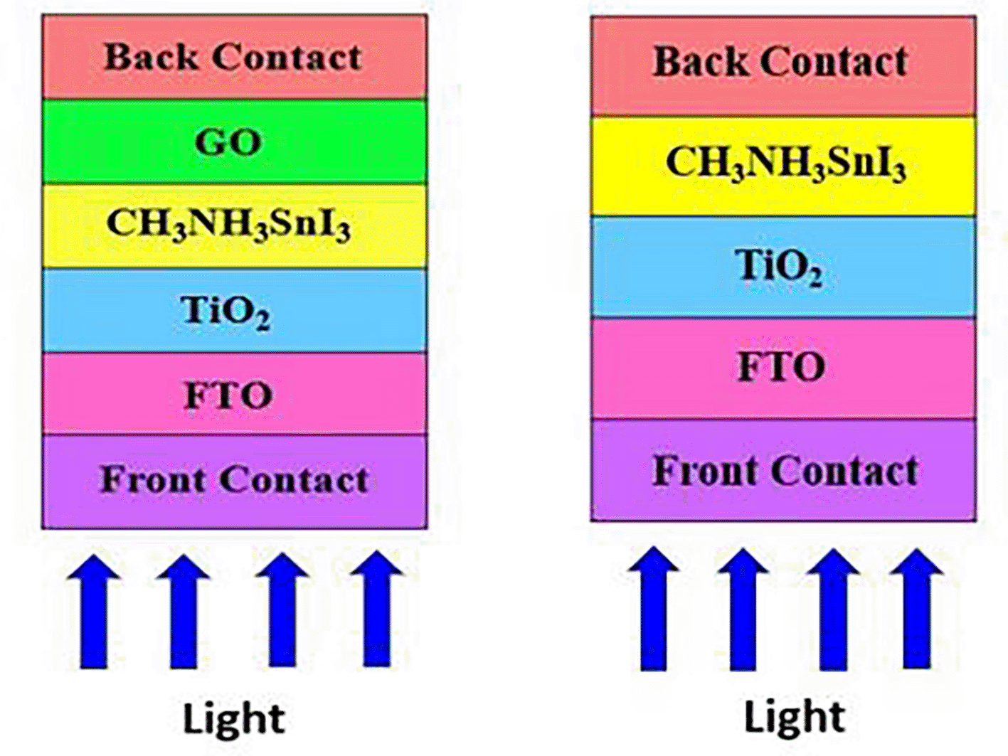
In the present work, two solar cell structures, one with HTL (D1) and the other HTL-free (D2), were simulated using CH3NH3SnI3 as the perovskite absorber layer using SCAPS 1D software. Within the scope of this study, a detailed investigation was conducted to scrutinize the impact of several influential parameters on the photovoltaic characteristics of two device structures, D1(GO/CH3NH3SnI3/TiO2/FTO (Fluorine doped tin oxide)) and D2 (CH3NH3SnI3/TiO2/FTO). For the D1 structure, the parameters include variations in the thickness, acceptor density, defect density of the hole transport and perovskite layer, interface defect density at the HTL/perovskite layer interface, variations in series and shunt resistance, and fluctuations in the operating temperature of the cell. For the D2 structure, the impact of variations in the thickness, acceptor density, defect density of the absorber layer, series and shunt resistance of the cell, and temperature on the device performance were considered. Furthermore, a comparative analysis was performed for the above two structures to study the impact of the GO layer on device performance.
Prior to the actual fabrication process, it is beneficial to conduct simulations of the proposed solar-cell structure to obtain an estimation of its expected performance and perform reliability analyses. This proves beneficial given the complex and time-consuming process involved in manufacturing solar cells, while also reducing both the associated risks and costs. Several software programs are available, including SILVACO ATLAS, COMSOL, SETFOS, AMPS, Wx-AMPS, and SCAPS-1D, which enable the simulation of solar cell characteristics based on input device parameters.
The SCAPS-1D software for numerical simulation was developed by the Department of Electronics and Information Systems, Ghent University, Belgium. Its primary function is to simulate the properties of the device by solving three key equations: Poisson's equation, electron/hole transport equation, and continuity equation. This facilitates the simulation of various device configurations and offers the capability of performing multiple batch runs for consistent data collection. In addition, it includes powerful tools for data analysis and visualization via user-friendly graphical interfaces.
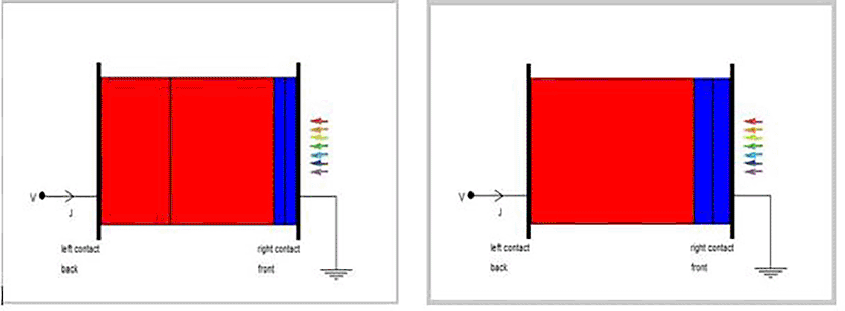
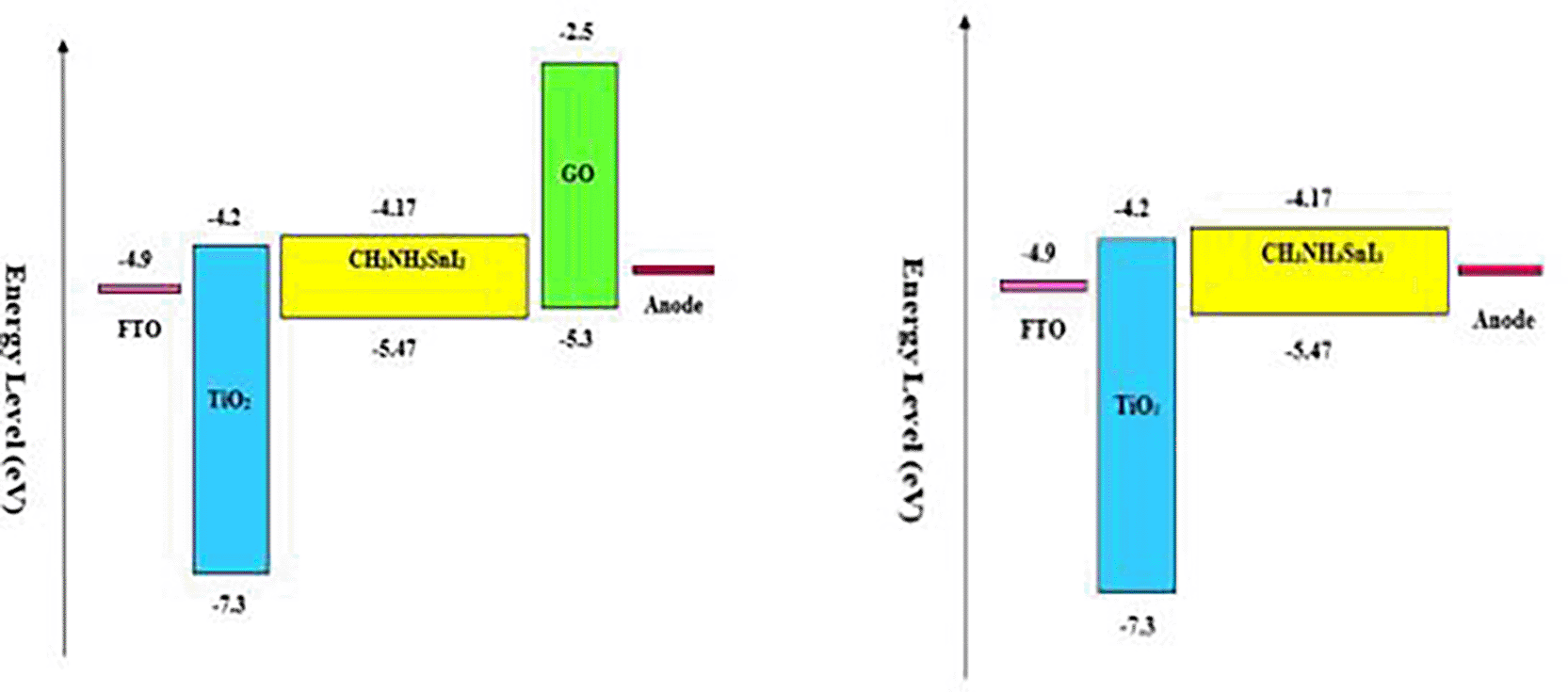
The SCAPS-1D software is capable of solving continuity equations for charge carriers, including the equation for hole continuity and electron continuity. Furthermore, it handles the optical absorption coefficient, overall charge transport, electron transport, and hole transport equations.5 Figure 1 and Figure 2 illustrate the solar cell definition panel and design of solar cell structures for D1 and D2 device structures respectively. Architecture of both the designed models are shown in Figure 3 followed by the energy band diagrams for both the device structures in Figure 4.
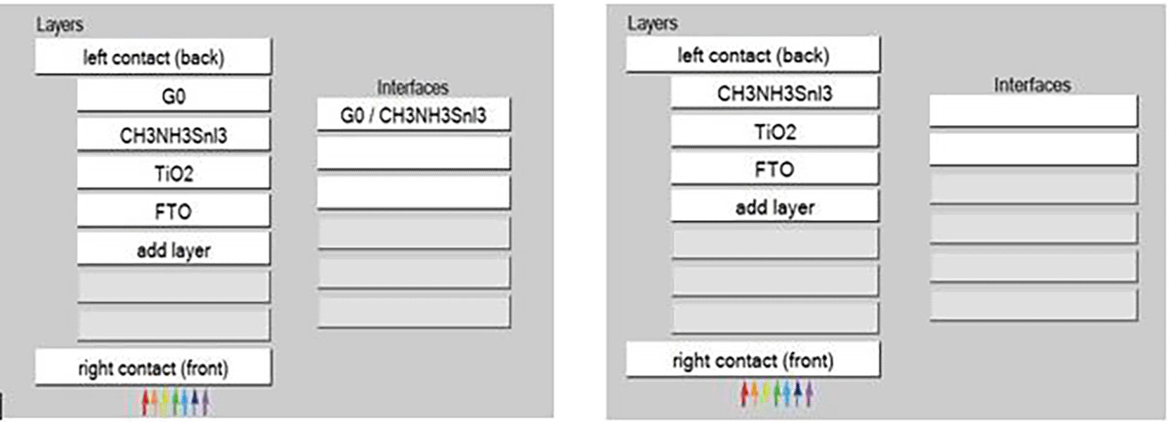
In this study, a simulation was conducted for two different device structures, namely D1 and D2. Device D1 encompassing a specific HTL that is Graphene Oxide, which was chosen to assess its compatibility with titanium dioxide (TiO2) as an ETL, along with CH3NH3SnI3 as the absorber layer, was optimized by varying the thickness, acceptor density, defect density of both the absorber layer and HTL, and defect density at the interface between the HTL and the perovskite layer. Another model, D2, encompassing CH3NH3SnI3 as the absorber layer without including any HTL was optimized by varying the thickness, acceptor density, and defect density of the absorber layers. Furthermore, adjustments were made to other PV parameters of the cell for both device models, such as series and shunt resistance and operating temperature. The aim is to identify the optimal conditions for achieving the highest possible device performance for both designed models through a simulation study. The properties of each layer were referenced from existing literature. The input parameters for the different layers are listed in detail in Tables 1 and 2.
| Parameters | GO3 | CH3NH3SnI39 | TiO29 | FTO9 |
|---|---|---|---|---|
| Thickness (nm) | 300 | 450 | 50 | 50 |
| Bandgap, Eg (eV) | 2.48 | 1.3 | 3.2 | 3.4 |
| Electron Affinity (eV) | 2.3 | 4.17 | 4.1 | 4.5 |
| Relative Permittivity, εr | 10 | 8.2 | 9 | 9.1 |
| CB density of states (1/cm3) | 2.2×10¹⁸ | 1×10¹⁸ | 2.2×10¹⁸ | 1.1×10¹⁹ |
| VB density of states (1/cm3) | 1.8×10¹⁹ | 1×10¹⁸ | 1.8×10¹⁹ | 1.1×10¹⁹ |
| Electron Thermal Velocity (cm/s) | 5.2×10⁷ | 1×10⁷ | 1×10⁷ | 1×10⁷ |
| Hole Thermal Velocity (cm/s) | 5×10⁷ | 1×10⁷ | 1×10⁷ | 1×10⁷ |
| Electron Mobility, μe (cm2/Vs) | 2.6×101 | 2×10³ | 5×10⁻² | 2×101 |
| Hole Mobility, μh (cm2/Vs) | 1.23×10² | 3×10² | 5×10⁻² | 1×101 |
| Donor Concentration, ND (1/cm3) | 0 | 0 | 1×10¹⁸ | 1.1×10¹⁹ |
| Acceptor Concentration, NA (1/cm3) | 4×10²⁰ | 7×10¹⁷ | 0 | 0 |
| Parameters | HTL/Perovskite3,6 |
|---|---|
| Defect Type | Neutral |
| Capture cross section electron (cm2) | 1.0×10⁻¹⁹ |
| Capture cross section holes (cm2) | 1.0×10⁻¹⁹ |
| Energetic Distribution | single |
| Reference for defect energy level Et | above the highest EV |
| Energy with respect to a Reference (eV) | 0.600 |
| Total Density (1/cm2) | 1.0×10⁹ |
3.1.1 Thickness
The basic role of the HTL in PSCs is to facilitate the transfer of holes from the perovskite layer to the electrode while also acting as a barrier between the perovskite layer and the electrode. The thickness of the HTL is crucial for optimal performance, because if the HTL is excessively thick, it increases the series resistance, impeding the efficient transfer of holes to the electrode. This can lead to a decrease in the overall cell performance. However, an HTL that is too thin may not provide sufficient separation between the perovskite layer and electrode.3 Consequently, this proximity can promote the recombination of charge carriers at the interface between the perovskite layer and the electrode, reducing the efficiency of the device. Therefore, finding the right balance in the thickness of the HTL is important to ensure efficient hole transfer and minimize recombination at the interface between the perovskite layer and the electrode in the cells.
Figure 5 illustrates the impact of adjusting the HTL thickness, ranging from 50 to 500 nm, on the resulting output parameters. The variation in the thickness of the HTL had a minimal impact on the photovoltaic parameters of the cell. Short-circuit current (JSC), efficiency (ɳ), open-circuit voltage (VOC) remained nearly unchanged, indicating that they were not significantly affected by the HTL thickness. Although there was a slight increase observed in the Fill Factor (FF) initially from 54.56 % to 54.57 % as HTL thickness was increased from 50 nm to 300 nm, the FF reverted to its initial value of 54.56 % within the range of HTL thickness from 350 nm to 500 nm. However, this small variation is considered negligible in practical terms, and does not have a meaningful impact on the overall performance of the cell.
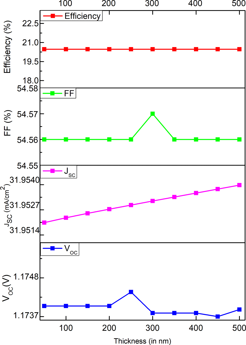
In summary, changes in photovoltaic parameters due to variations in the HTL thickness were minimal, indicating that the effect was insignificant at such levels of variation. Hence, 300 nm was taken as the optimal thickness for the HTL, resulting in Voc = 1.17 V, Jsc = 31.95 mA/cm2, FF = 54.57 %, and Efficiency = 20.47 %.
3.1.2 Acceptor density
To achieve the ideal acceptor density for doping the HTL, device simulations were conducted with varying HTL acceptor densities ranging from 1010 cm−3 to 1021 cm−3, while the acceptor density value of the absorber layer was fixed at 1×1014 cm−3 and the donor density value of the ETL was fixed at 1×1018 cm−3 respectively. The objective is to determine the doping density that would optimize the performance of PSC by striking a balance between the enhanced PV characteristics and minimizing any adverse effects on the device. Figure 6 provides a visual representation of the correlation between the doping concentration of GO and cell performance parameters. By increasing doping concentration from 1010 cm−3 to 1021 cm−3, notable improvement in PCE was observed, with PCE increasing from approximately 18 % to 22 %. This was due to the increase in the GO doping concentration, and the disparity between the energy bands of GO and the absorber layer became more pronounced. This leads to an enhanced electric potential, resulting in a stronger electric field that facilitates efficient separation of photogenerated carriers. Consequently, the recombination rate decreased, ultimately improving the overall performance of the cell.5 However, achieving doping concentrations higher than 1020 cm−3 for the hole transport layer is challenging. Hence, the optimal value was considered for an HTL doping concentration of 1020 cm−3.
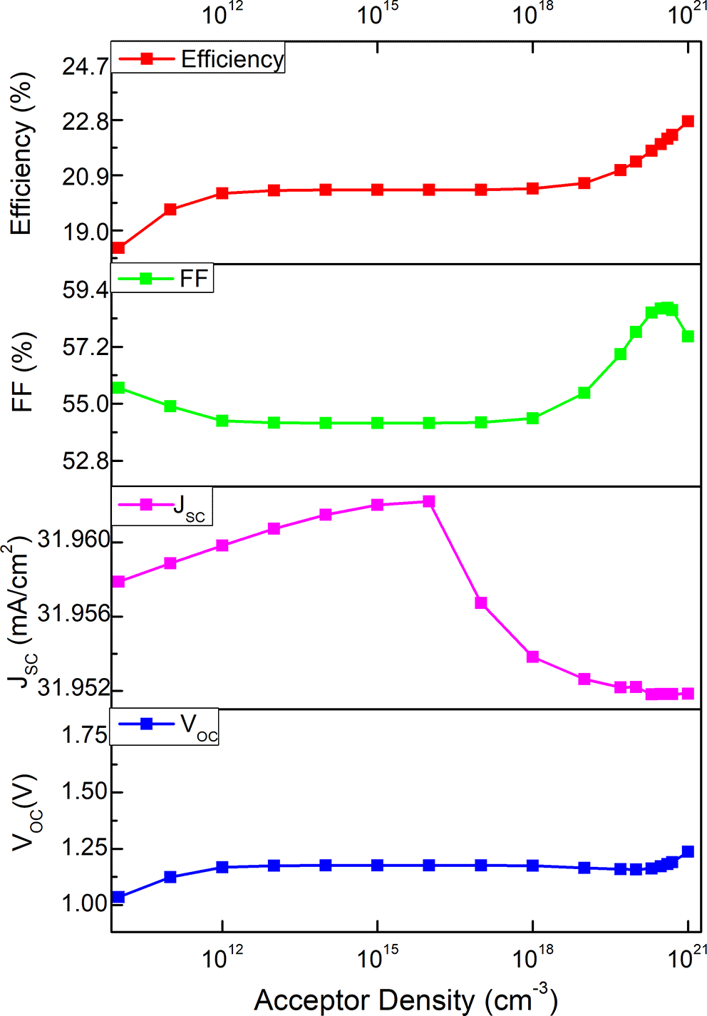
Moreover, a high density of acceptor dopants can create deep Coulomb traps, which can negatively affect the mobility of holes within the material.7 With a doping concentration of the hole transport layer of 4×1020 cm−3, the solar cell performance was coming a PCE of 22.15 %, FF of 58.70 %, Voc of 1.18 V, and Jsc of 31.95 mA/cm2.
3.1.3 Defect density
The defect density in the HTL of perovskite solar cells is an important parameter that affects the overall device performance. Defect density in HTL can arise from various sources, including impurities, lattice imperfections, and grain boundaries.8 To examine how the performance of the PSC is affected by changes in the defect values for the HTL, the defect values were varied in the range of 1010 cm−3 to 1020 cm−3. Figure 7 shows a plot of the fluctuation of the defect density in the HTL. However, as the defect density increased, there was a noticeable decrease in JSC. Defects in HTL can act as trap states for charge carriers, leading to increased recombination rates.8 Recombination refers to the loss of photogenerated electrons and holes before they can contribute to the photocurrent. Defects in the HTL hinder the efficient transport of charge carriers, specifically holes, from the perovskite layer to the electrode.9 This can result in lower hole mobility and decreased charge extraction, leading to a reduced photocurrent and overall device performance. Furthermore, defects in the HTL can introduce additional resistance into the device, particularly in the series resistance pathway. This increased series resistance can impede the flow of charge carriers, leading to a reduction in the photocurrent and Jsc. Therefore, increasing the defect density in the HTL of a cell is generally expected to decrease Jsc owing to the increased recombination, hindered charge transport, and increased series resistance.
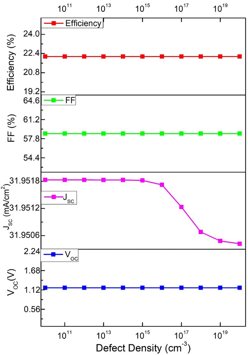
Hence, optimizing the HTL and minimizing the defect densities are critical for improving the efficiency and stability of perovskite solar cells. According to present simulation studies, the cell exhibits optimal performance at a defect density of Nt = 1012 cm−3, resulting in JSC = 31.95 mA/cm2, VOC = 1.18 V, FF = 58.70 %, PCE = 22.15 %.
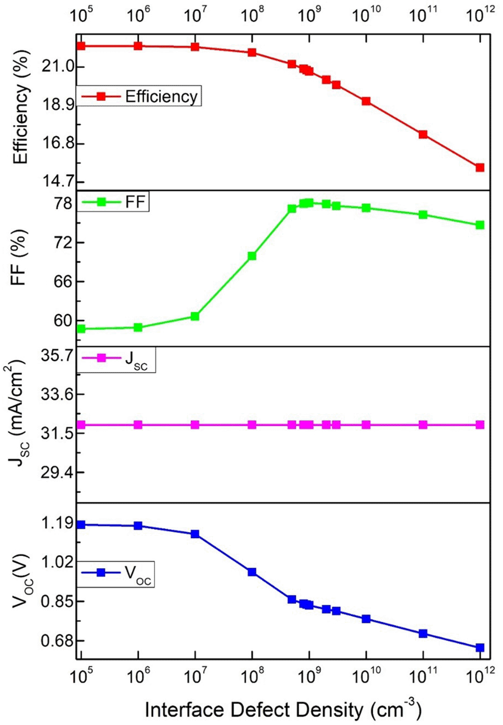
3.1.4 Interface defect density of HTL/Active layer
The interface plays a vital role in the performance of photovoltaic devices, as it directly affects the recombination of electrons and holes.3 To examine the impact of defects at the interface between GO and CH3NH3SnI3, the performance of the cell was analysed by varying the defect densities from 105 cm−3 to 1012 cm−3. As depicted in Figure 8, the JSC remained constant, while the VOC experienced a significant decrease from 1.18 V at 105 cm−3 to 0.64 V at 1012 cm−3. As the defect density at the interface increased, the FF of the photovoltaic device exhibited an upward trend until it reached a threshold of approximately 109 cm−3. However, the PCE of the device continued to decrease from 22.15 % at 105 cm−3 to 15.49 % at 1012 cm−3. An elevated level of interface defects at the interface leads to an increase in trapping and recombination sites, thereby diminishing device performance.3 The occurrence of excess carrier density at the HTL/perovskite interface leads to an amplified charge recombination process.3 Thus, prioritizing the improvement of the GO/perovskite interface quality by minimizing the interface defects in the region requires significant attention. Based on the simulation study, for GO/perovskite interface, the density of interface defects needs to be 109 cm−3 to achieve enhanced results, with an FF of 78.07 % and a PCE of 20.76 %.
3.2.1 Thickness
The choice of absorber layer thickness is a trade-off between light absorption and charge collection efficiency. A thicker absorber layer can absorb more light because of its higher photon absorption, resulting in increased photocurrent generation. However, it can also lead to a longer path for charge carriers to travel, potentially increasing the charge recombination losses.10 However, a thinner absorber layer reduces the path length for charge carriers, thus enhancing the charge collection efficiency. However, this may limit the amount of light absorbed and decrease the overall photocurrent. Optimizing the absorber layer thickness involves finding a balance between maximizing the light absorption and minimizing the charge carrier transport losses.10
To determine the optimal thickness of the absorber layer, simulations were conducted over a range of 100–1000 nm for both device structures D1 and D2 while keeping the other parameters constant. The dependence of the performance parameters on the thickness of the absorber layer is shown in Figure 9.
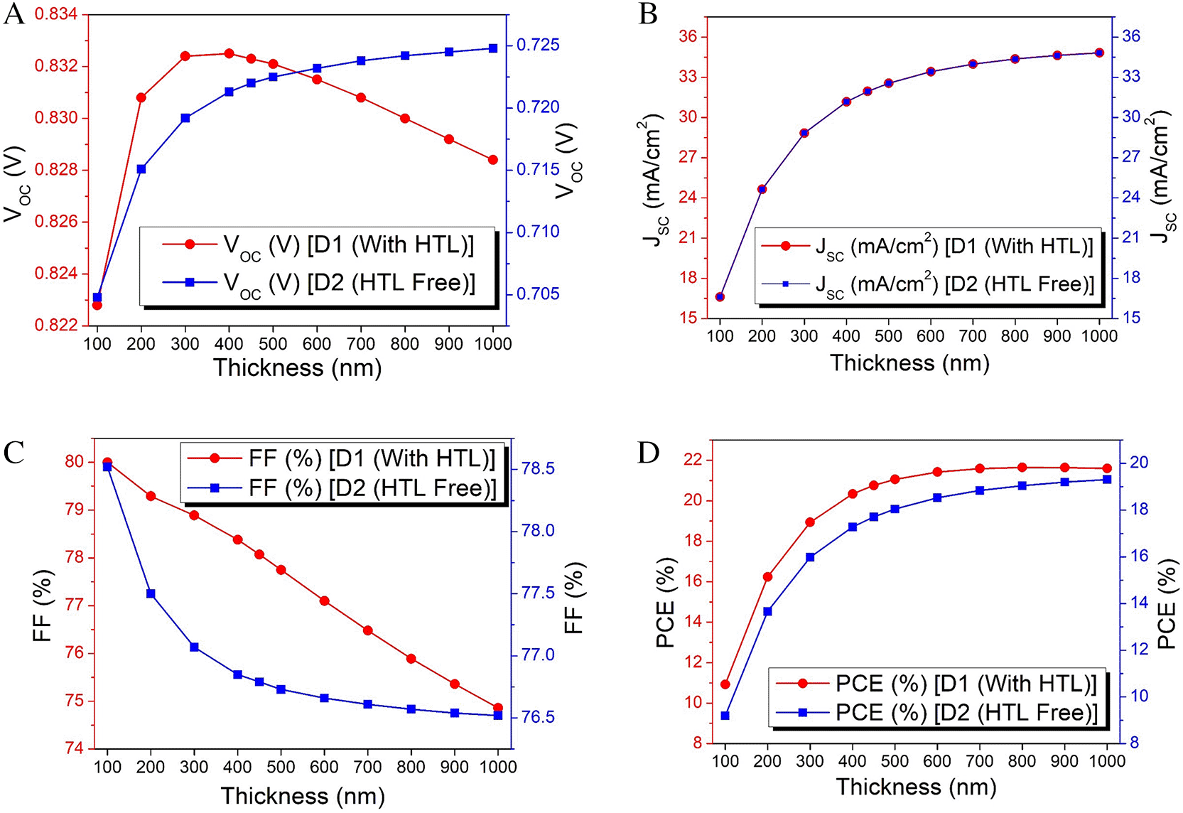
As shown in Figure 9(b), increasing the absorber layer thickness leads to increasing values of JSC for D1 and D2. The increase in JSC can be attributed to the greater absorption of photons as the absorber layer thickness increases. With a thicker absorber layer, more photons are absorbed, resulting in an increase in the excess carrier concentration, which consequently leads to an increase in JSC.11
Conversely, when the absorber layer thickness increased, the series resistance within the cell and its internal power depletion also increased. This, in turn, causes a continuous decrease in FF, which is evident in both D1 and D2.11
Voc can be determined using the following equation:
As the absorber layer thickness decreased, the recombination of electrons and holes decreased, leading to a decrease in the reverse saturation current (Io). Meanwhile, as the thickness of the absorber layer increased, the concentration of excess carriers also increased, resulting in an increase in the photocurrent (IL) and subsequent enhancement of the open-circuit voltage (Voc).11 Figure 9(c) clearly shows that for D2, the values of VOC continued to increase with increasing absorber layer thickness. For D1, the VOC increases to an optimal value of 0.83 V when the thickness is 450 nm. After reaching this optimal value, Voc reached a saturation point with minimal decrease. However, the decline in Voc was not significant.12
The PCE of the cell can be determined by the combined effects of the Voc, Jsc, and FF.
By extracting the values of Jsc, Voc, and FF from the results depicted in the Figures, it is evident that as the thickness increased, the PCE also increased for both D1 and D2. This observation can be deduced by substituting the obtained values into (2).12 Thus, 450 nm can be considered as the optimal thickness for D1 and D2, yielding the following set of PV parameters Voc = 0.83 V, Jsc =31.95 mA/cm2, FF=78.07 %, Efficiency=20.76 % (for D1 structure) and Voc = 0.72 V, Jsc =31.94 mA/cm2, FF=76.79 %, Efficiency=17.71 % (for D2 structure) respectively.
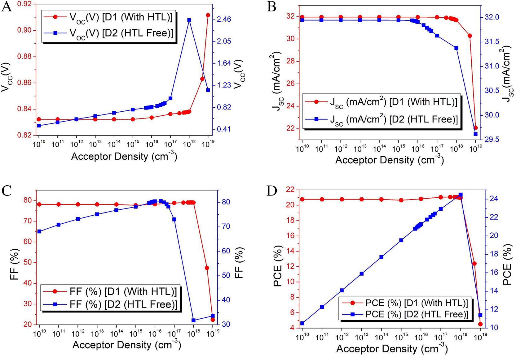
3.2.2 Acceptor density
The acceptor concentration in a tin-based perovskite absorber layer refers to the doping of perovskites with acceptor-type dopants. In doping, impurities are intentionally introduced into the crystal lattice of a material to modify its properties. In the context of perovskite solar cells, acceptor doping typically involves introducing cations that are electron-deficient, leading to p-type conductivity. Acceptor doping can be used to tune the electrical properties of perovskite materials, such as their conductivity and charge carrier concentration, which in turn affect the overall performance of the solar cell. The acceptor densities of the absorber layers of the two structures were investigated by varying them within the range of 1010 cm−3 to 1019 cm−3 as illustrated in Figure 10. With an acceptor density of 1010 cm−3, the open-circuit voltage is 0.83 V, while at 1019 cm−3, it rises to 0.91 V for D1. This increase in VOC can be attributed to the declining Fermi level of holes with increasing acceptor density.9 For D2, at an acceptor density of 1010 cm−3, open-circuit voltage is 0.48 V and it keeps on rising with increase in acceptor density value, reaches maximum that is 2.45 V at 1018 cm−3. However, beyond this value, the plot of Voc started declining. The graph for JSC exhibits a declining pathway with the current density decreasing from 31.95 mA/cm2 at 1010 cm−3 to 22.08 mA/cm2 at 1019 cm−3 for D1 and from 31.94 mA/cm2 at 1010 cm−3 to 29.61 mA/cm2 at 1019 cm−3 for D2. This behaviour was attributed to the increased recombination of charge carriers at higher acceptor densities.9 As acceptor density increased from 1010 cm−3 to 1019 cm−3, graph for Fill Factor exhibited declining trend, dropping from approximately 78 % to nearly 22 % for D1 and from approximately 68 % to nearly 33 % for D2 respectively. This decrease in the Fill Factor is associated with an increase in the charge-carrier recombination rate within the absorber layer.9 Increased acceptor concentrations can lead to detrimental effects on charge carrier transport, recombination rates, and other optoelectronic properties, thereby reducing the efficiency of the solar cell, as is evident from the efficiency plots of the two devices.9 The analysis reveals that the simulated solar cell demonstrates the finest performance outcomes with Voc = 0.84 V, Jsc = 31.77 mA/cm2, FF = 79.04 %, Efficiency = 21.04 %, when acceptor density of absorber layer is set to 7×1017 cm−3 for D1 and with Voc = 0.84 V, Jsc = 31.84 mA/cm2, FF = 80.56 %, Efficiency = 21.78 %, when the acceptor density of absorber layer is set to 2×1016 cm−3 for D2.
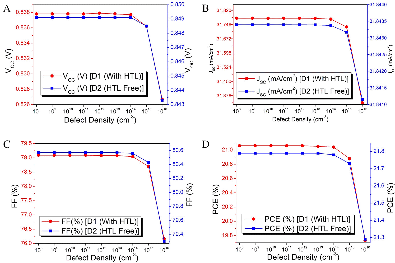
3.2.3 Defect density
The defects present in an absorber layer, both in terms of their type and quantity, lead to nonradiative recombination, which significantly affects the performance of the device. Figure 11 shows the performance parameter curves of the two cells for different defect densities ranging from 108 cm−3 to 1016 cm−3. This Figure clearly illustrates a significant reduction in the performance parameters as the defect density (Nt) increases. For D1, at Nt = 108 cm−3, Jsc = 31.78 mA/cm2, Voc = 0.84 V, PCE = 21.06 %, FF = 79.09 % and when Nt = 1016 cm−3, Jsc = 31.34 mA/cm2, Voc = 0.83 V, PCE = 19.73 %, FF = 76.16 %. For D2, at Nt = 108 cm−3, Jsc = 31.84 mA/cm2, Voc = 0.84 V, PCE = 21.79 %, FF = 80.57 % and when Nt = 1016 cm−3, Jsc = 31.84 mA/cm2, Voc = 0.84 V, PCE = 21.29 %, FF = 79.30 %. Observing this data, it becomes evident that as the defect density increases, there is a noticeable decrease in all the above parameters for both cells. The decrease in performance with increasing defect density is primarily attributed to the recombination process, resulting in the annihilation of charge carriers.10 When the defect density was low, the carrier diffusion length was greater, leading to a reduced recombination process.10 Consequently, this condition contributes to improved PV performance. The most favourable outcome is achieved at a Nt of 1010 cm−3 with Jsc = 31.78 mA/cm2, Voc = 0.84 V, PCE = 21.06 %, FF = 79.09 % for D1 and Nt of 1011 cm−3 with Jsc = 31.84 mA/cm2, Voc = 0.84 V, PCE = 21.79 %, FF = 80.57 % for D2.
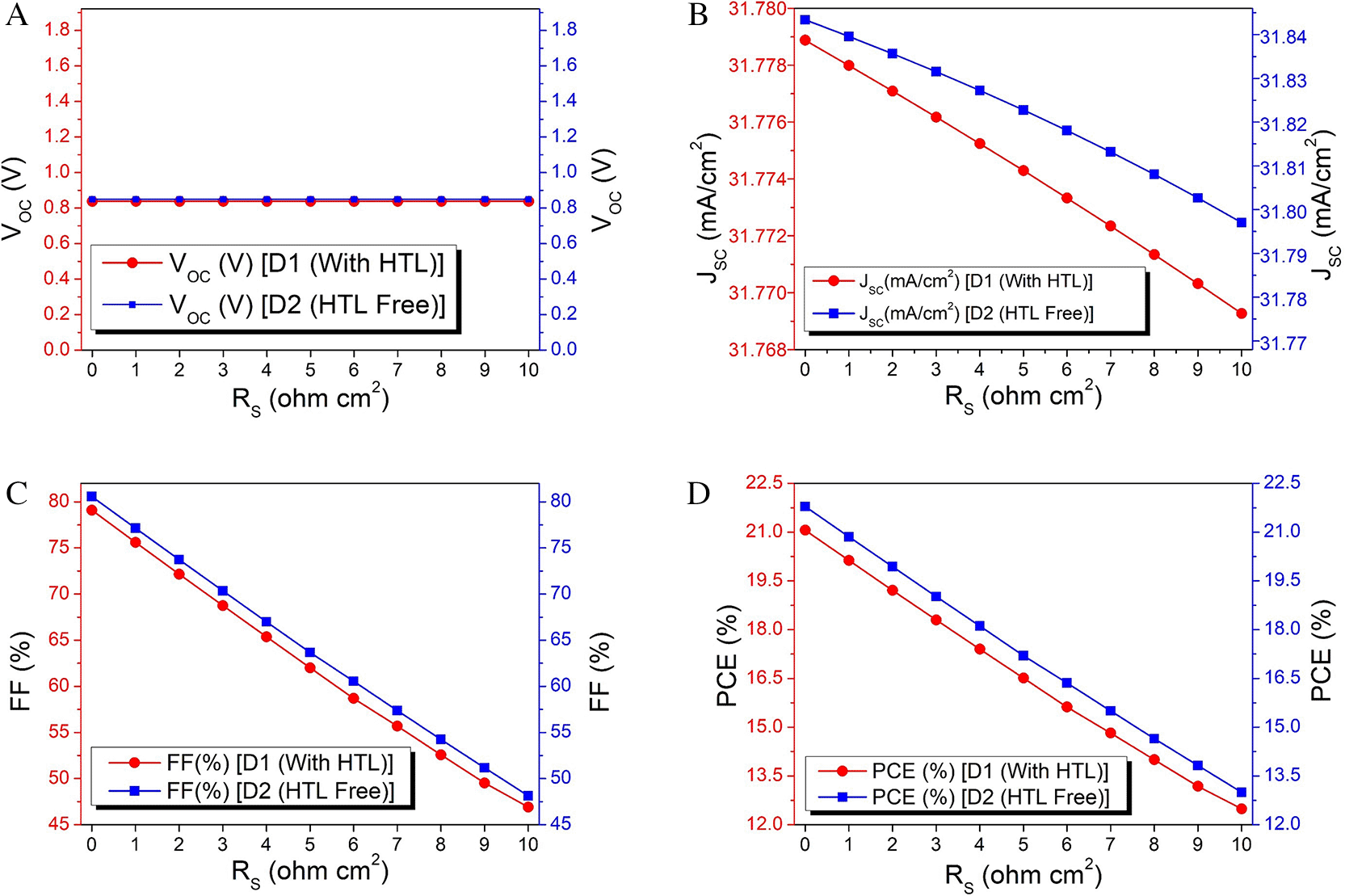
The components of a PSC, namely the HTL, perovskite layer, ETL, and front contact (FTO), introduce electrical resistance to the device. To investigate the impact of the series resistance on the PSCs performance, simulations were conducted by varying the series resistance from 0 Ω cm2 to 10 Ω cm2 for both device structures. The results, as shown in Figure 12, reveal that the open-circuit voltage remained unchanged with the variation in series resistance for D1 and D2, while other parameters such as short-circuit current, fill factor, and power conversion efficiency decreased with higher series resistance for both D1 and D2. Hence, it is evident that a lower series resistance value is preferable for achieving better overall PSC performance.13,14 Consequently, a series resistance value of 1 Ω cm2 is considered the optimal choice for both the structures, resulting in a fill factor of 75.60 % (D1), 77.15 % (D2) and an efficiency of 20.13 % (D1), 20.86 % (D2).
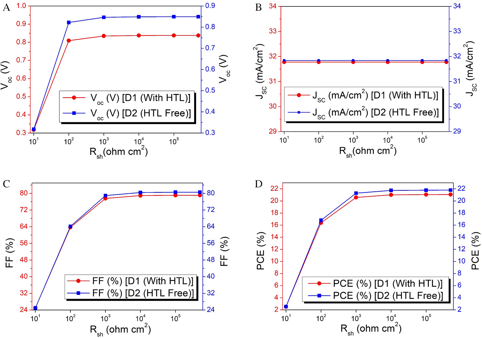
The presence of various charge recombination paths in PSC leads to a shunt resistance.13 To investigate the impact of shunt resistance on the device performance, simulations were conducted by varying the shunt resistance from 1×101 Ω cm2 to 5×10⁵ Ω cm2. Figure 13 shows the variation in the device parameters with different shunt resistance values for the D1 and D2 devices. Notably, the efficiency and fill factor of both PSCs exhibit significant improvements with increasing shunt resistance.14 At a shunt resistance of 5×10⁵ Ω cm2, both the PSCs demonstrated an impressive power conversion efficiency of 21.06 % (D1); 21.79 % (D2), and a high fill factors of 79.09 % (D1); 80.57 % (D2). Thus, 5×10⁵ Ω cm2 is taken as the optimal shunt resistance for the D1 and D2 structures; at this value, the cell delivers enhanced performance in terms of efficiency and fill factor.
Solar cells tend to operate more efficiently at 300 K, which corresponds to room temperature, than at higher temperatures. To investigate the impact of the operating temperature on the performance of the proposed cells, variations in temperature ranging from 296 to 400 K were employed, as illustrated in Figure 14. With increasing temperature, the plots of Voc, Jsc and efficiency show an upward trend for the D1 structure. However, the plot for FF shows an upward trend until 306 K; thereafter, the plot shows degradation with a further increase in temperature. This can be attributed to the fact that, with an increase in temperature, electrons experience heightened instability owing to the influx of greater energy. Consequently, their recombination with holes becomes more challenging when they enter the charging zone, resulting in lower FF.9
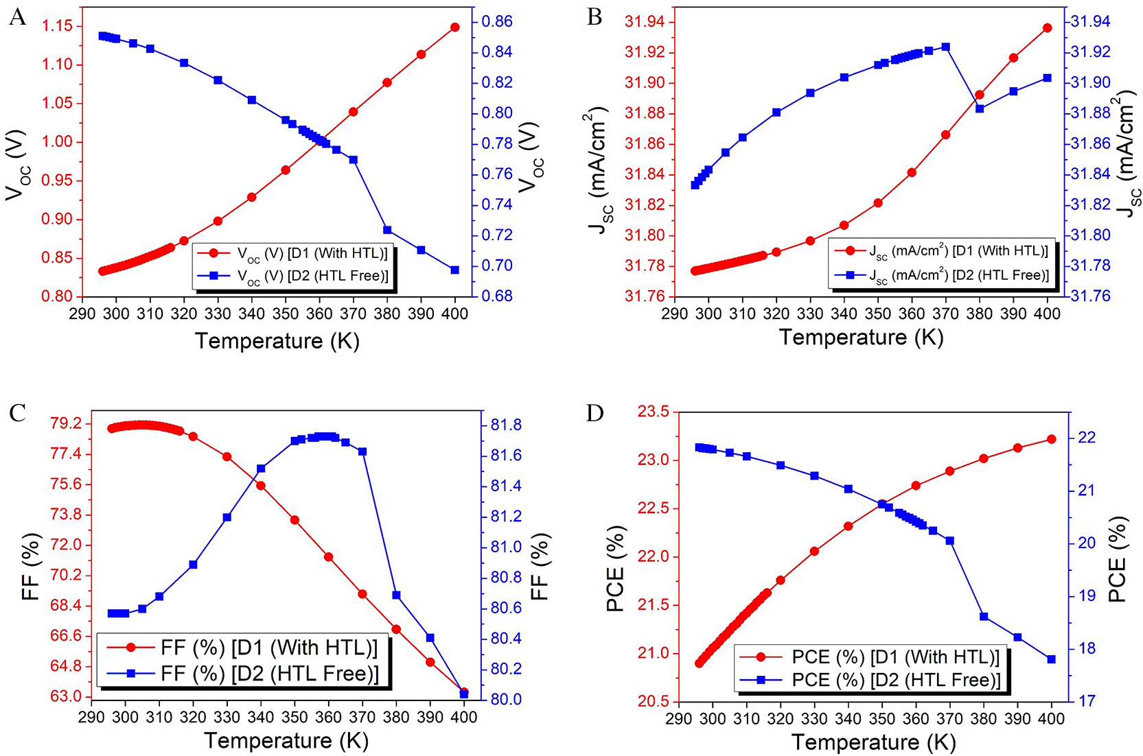
For D2, with an increase in temperature, the plot of Voc and PCE followed a downward trend. However, the plot for FF shows an upward trend until 360 K, and thereafter, the plot degrades with a further increase in temperature. The decrease in the output values observed with increasing temperature occurs because the electrons receive additional energy, rendering them highly unstable. Consequently, they encounter difficulties recombining with holes as they reach the charging zone.15 Although the value of Jsc diminishes to some extent, it subsequently increases with increasing temperature. This phenomenon is attributed to the decrease in the band gap energy, which facilitates the generation of a greater number of hole-electron pairs from high-energy photons.15
The simulation indicates that the cell D1 achieves its most optimal performance characteristics at a temperature of 306 K with Voc = 0.85 V, Jsc = 31.78 mA/cm2, FF = 79.14 %, Efficiency = 21.28 % and the cell D2 attains its peak performance at a temperature of 357 K with Voc = 0.78 V, Jsc = 31.91 mA/cm2, FF = 81.73 %, Efficiency = 20.52 %.
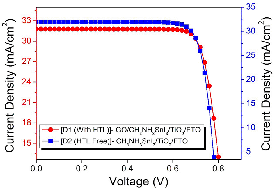
The two solar cells were simulated using their finely tuned parameters. Device structure D1 includes a 450 nm thick absorber layer featuring an acceptor density of 7×1017 cm−3 and a defect density of 1×1010 cm−3. Additionally, a 300 nm thick HTL was employed, which was characterized by an acceptor density of 4×1020 cm−3 and a defect density of 1×1012 cm−3. The HTL/perovskite interface defect density was set at 1×109 cm−3, and the simulation was conducted at an operating temperature of 306 K. On the other hand, the device structure D2 included a 450 nm thick absorber layer featuring an acceptor density of 2×1016 cm−3 and a defect density of 1×1011 cm−3, and the simulation was conducted at an operating temperature of 357 K. The resulting JV curve, depicted in Figure 15, was generated from the simulation of the above two models. The simulated cell D1 exhibited optimal key characteristics like short-circuit current density 31.78 mA/cm2, efficiency 21.28 %, fill factor 79.14 % and open-circuit voltage 0.84 V and the simulated cell D2 exhibited optimal key characteristics like short-circuit current density 31.91 mA/cm2, efficiency 20.52 %, fill factor 81.73 % and open-circuit voltage 0.78 V.
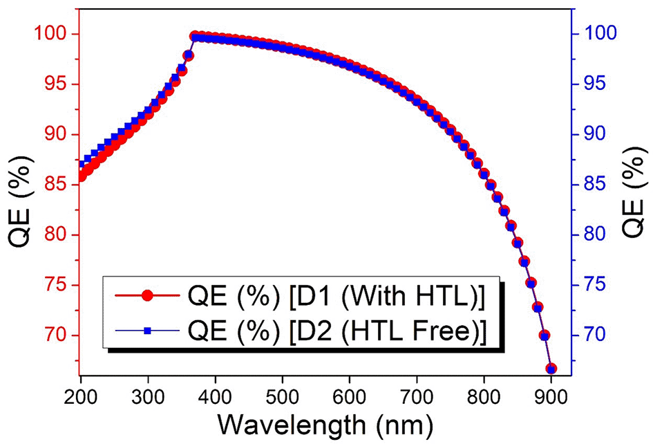
The effectiveness of a solar cell is evaluated using two key metrics: external quantum efficiency (EQE) and internal quantum efficiency (IQE). The EQE considers the optical performance of the solar cell and the ratio of charge generation relative to the incident light photons. Conversely, IQE measures the ratio of electrons collected as a photocurrent to the number of absorbed photons at a specific wavelength. The IQE is useful for estimating the total current generation across the solar spectrum and determining the range of the solar spectrum utilized for power generation by the active material. However, EQE may be subject to future analysis for a more in-depth examination.16
The external quantum efficiencies (EQE) of the two devices were observed, providing insights into the effectiveness of carrier generation from incident photons at specific wavelengths. Figure 16 illustrates the spectral dependence of QE for the proposed device structures within the wavelength range of 200–900 nm. The Peak spectral responses were achieved around 99.77 % QE for D1 and 99.64 % QE for D2 at 370 nm, which is in the visible range.
In this study, we introduce two basic models for lead-free PSCs. The GO/CH3NH3SnI3/TiO2/FTO configuration, which is the D1 device structure, notably includes CH3NH3SnI3 as the perovskite absorber layer and GO as the HTL. In contrast, the configuration CH3NH3SnI3/TiO2/FTO, which is a D2 device structure, is essentially HTL-free, comprising CH3NH3SnI3 as the perovskite absorber layer. A thorough comprehensive SCAPS-1D simulation ascertain that the cells possess the capability to achieve good efficiency along with an impressive fill factor under optimal conditions that is ɳ = 21.28 %; FF = 79.14 % for D1 and ɳ = 20.52 %; FF = 81.73 % for D2. The optimization process of the cell was explored by varying certain parameters for the absorber layer as well as the HTL in the case of D1, and by varying a few parameters for the absorber layer in the case of D2. After subjecting both devices to diverse conditions, it becomes evident that the photovoltaic attributes are contingent on several other factors such as quantum efficiency, series resistance, shunt resistance, and operating temperature, and altering these factors produces a range of output results. The study reveals that upon proper optimization of parameters; the photovoltaic characteristics of the cells are enhanced. Consequently, the proposed models generate an overall performance profile of Voc = 0.84 V, Jsc = 31.78 mA/cm2, FF = 79.14 %, and ɳ = 21.28 % for D1 and Voc = 0.78 V, Jsc = 31.91 mA/cm2, FF = 81.73 %, and ɳ = 20.52 % for D2. Notably, the proposed approach sidesteps lead toxicity by employing Sn-based perovskite structures. It can be analysed that, D2 resembles an uncomplicated simple architecture involving minimum number of input layers and is thus cost effective. However, the model with the HTL, that is, D1- GO/CH3NH3SnI3/TiO2/FTO, has the potential to yield a stable FF by facilitating hole extraction and reducing energy barriers, thus resulting in a reduced rate of recombination. Comparing the performance of the two models, it can be concluded that the efficiency obtained in the case of D1 is comparatively higher than that obtained for D2, and D1 exhibits a consistently stable fill factor, which can be attributed to the use of HTL in this device model. Given these merits, the suggested device structure holds promise for experimental realization, propelling the domain of Pb-free PSCs forward.
| Views | Downloads | |
|---|---|---|
| F1000Research | - | - |
|
PubMed Central
Data from PMC are received and updated monthly.
|
- | - |
Provide sufficient details of any financial or non-financial competing interests to enable users to assess whether your comments might lead a reasonable person to question your impartiality. Consider the following examples, but note that this is not an exhaustive list:
Sign up for content alerts and receive a weekly or monthly email with all newly published articles
Already registered? Sign in
The email address should be the one you originally registered with F1000.
You registered with F1000 via Google, so we cannot reset your password.
To sign in, please click here.
If you still need help with your Google account password, please click here.
You registered with F1000 via Facebook, so we cannot reset your password.
To sign in, please click here.
If you still need help with your Facebook account password, please click here.
If your email address is registered with us, we will email you instructions to reset your password.
If you think you should have received this email but it has not arrived, please check your spam filters and/or contact for further assistance.
Comments on this article Comments (0)